

GD32F103RET6 Complete Specs & Pinout Guide with Circuit Tips
The GD32F103RET6 ships with a Cortex-M3 core running up to 108 MHz and packs 512 KB Flash and 64 KB SRAM, spec numbers that make it a strong choice for mid-range embedded applications. This guide walks firmware engineers, hardware designers, and makers through full specs, a clear LQFP64 pinout overview, and practical circuit tips to wire, power, and debug a board quickly and reliably.
Readers will find focused, actionable recommendations for power, decoupling, clocking, USB and CAN interfaces, and common troubleshooting steps. The intent is a single reference that pairs data-driven guidance with hands-on tips so you can move from schematic to working prototype with fewer iteration cycles.
Background & Where this MCU Fits
MCU family positioning and typical use cases
This device targets general-purpose 32-bit embedded systems that need higher performance than small Cortex‑M0 parts but without the complexity of high-end parts. Typical use cases include USB device endpoints, CAN network nodes, motor control and mid‑range data acquisition where deterministic timers, DMA and multiple comms interfaces speed development while keeping BOM and power modest.
At-a-glance specs summary
Top-line specifications to keep on the first page of any quick reference: core Cortex‑M3; max CPU frequency 108 MHz; Flash 512 KB; SRAM 64 KB; package LQFP64; maximum I/O count ≥51. These items are the baseline for deciding if the device meets code size, RAM, timing and pin density needs before diving into peripheral details.
Complete Technical Specs (data deep-dive)
Performance Visualization
Memory, clock, and core details
The Cortex‑M3 core delivers deterministic interrupt latency and rich debug support. Typical clock architecture includes a main PLL that multiplies an external or internal oscillator up to the documented 108 MHz core clock; Flash access and wait‑state behavior affects attainable system clock and code execution timing. Verify datasheet tables for Flash wait states at each clock rate and plan DMA and ISR timing around those constraints.
Peripherals, ADC/DAC, timers, comms and IO
Peripherals include multi-channel ADCs (common sample-time tradeoffs), no dedicated DAC on many variants, several general‑purpose and advanced timers for PWM, USB Full Speed device support, CAN 2.0B interface, multiple UART/USART, SPI, I2C and I2S channels, DMA controllers, RTC and watchdogs. When designing, consider ADC sample time vs input source impedance, USB FS timing requirements, and that CAN requires an external transceiver for bus signaling and termination.
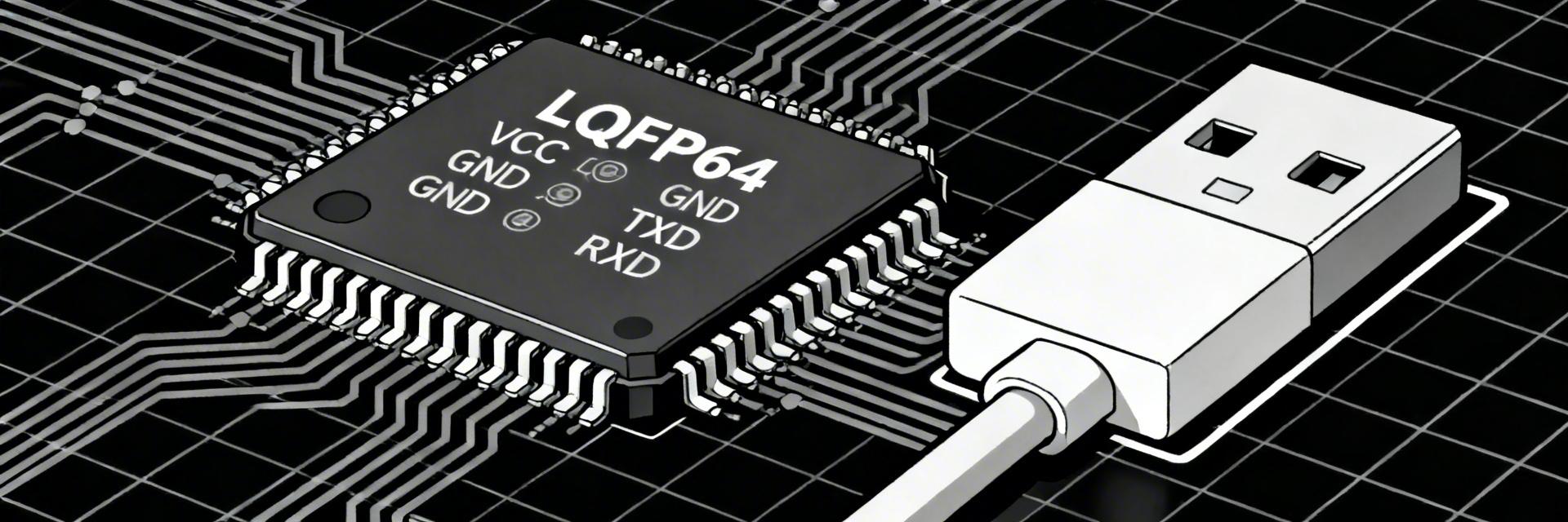
Pinout & Package Guide (LQFP64)
LQFP64 pin mapping: key pins to call out
A proper LQFP64 pinout diagram highlights power pins (VDD, VSS), NRST, BOOT0, VREF+/VREF-, USB D+/D-, CAN RX/TX, and the oscillator pins. Include grouping guidance for VDD pins and ground vias under the device for thermal and noise reasons. For production art, provide a labeled SVG/PNG showing pin numbers and names from the official pin table so assemblers and firmware teams share a single canonical reference.
Alternate functions & typical pin wiring patterns
Alternate function mapping uses AF registers and remap bits; plan pin usage early to avoid conflicts between UARTs, SPI clusters and timers. Common wiring patterns: place UART TX/RX pairs on adjacent pins if board routing allows, cluster SPI pins to minimize trace crossings, and route USB D+/D- as a matched differential pair. Provide a simple table mapping pins to primary functions and recommended pull (up/down/none) to streamline schematic reviews.
Circuit Design Tips & Reference Schematics
Power supply, decoupling and reset circuitry
Decoupling strategy: one 0.1 µF ceramic per VDD pin placed as close as possible to the pin, plus a 4.7–10 µF bulk on the board input near the regulator. Place VSS pads and vias beneath the package, and use a star ground for sensitive analog sections. Typical pull values: a 10 kΩ pull‑down or pull‑up on BOOT0 depending on desired default, and a 10 kΩ pull‑up on NRST if an active low reset is required; include an RC reset only if brown‑out timing needs smoothing.
USB, CAN, oscillator and analog front-end tips
USB FS routing requires a matched differential pair with controlled impedance, short stubs, and ESD protection near the connector. VBUS sense must be wired per the device’s input requirements and include a series resistor for filtering; use an external CAN transceiver with proper 120 Ω termination at each end of the bus and place common‑mode protection near the connector. For clocking, choose a crystal and loading caps per the oscillator recommendation when USB or CAN timing accuracy is critical; internal RC may suffice for non‑timing‑critical applications.
Debugging, Boot Modes & Practical Troubleshooting
Boot sequence & SWD
Understand BOOT0 state and the bootloader path to force system bootloader versus user flash. Wire SWD pins to a standard debug header with minimal routing length and clear silkscreen. When programming, be cautious with option bytes or protection bits that lock the Flash; plan an erase strategy for large images and provide a recovery path to restore devices bricked by errant firmware.
Diagnostic Checklist
Verify all power rails and regulator outputs, confirm reset pulse characteristics, check oscillator amplitude with a scope, and validate BOOT pin default state. For USB failures, inspect VBUS presence, D+/D- pull resistors, and clock accuracy. Use a simple LED blink test early to confirm core clock and vector table mapping before adding peripherals.
Summary
- • The GD32F103RET6 delivers a 108 MHz Cortex‑M3 with 512 KB Flash and 64 KB SRAM in LQFP64, offering a balanced mix of performance and peripherals for mid‑range USB/CAN applications; follow the pinout and power rules above to avoid common EMI and reset problems.
- • Adopt a decoupling plan of 0.1 µF per VDD and a 4.7–10 µF bulk cap, place VSS under the device, and use 10 kΩ pulls on BOOT0/NRST as typical starting values; these steps reduce debugging time and improve stability in production.
- • Route USB as a controlled differential pair, use an external CAN transceiver with proper termination, and prefer a crystal oscillator for bus‑timed interfaces; document pin alternate functions early to prevent remap conflicts during layout.
Frequently Asked Questions
How do I verify the GD32F103RET6 is powering up correctly? +
What are common causes of USB enumeration failures on this MCU? +
How should I approach recovering a board with bad firmware or locked Flash? +
