High-performance 108 MHz ARM Cortex-M3 microcontroller optimized for cost-sensitive embedded control and deterministic performance.
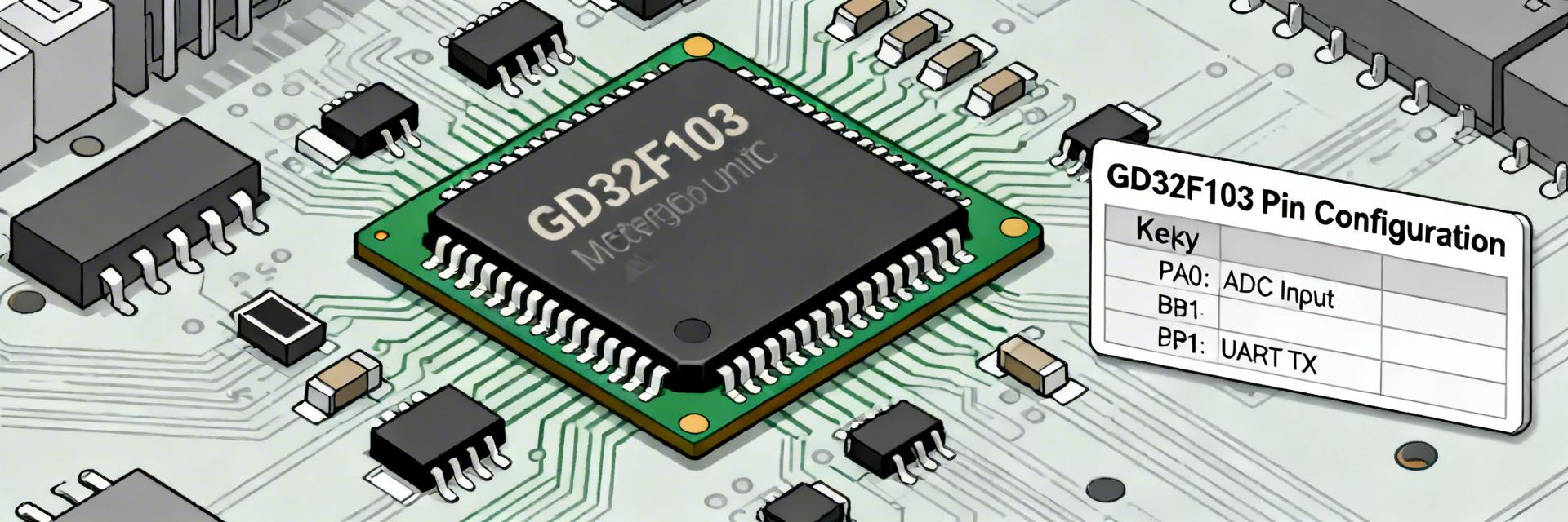
The GD32F103TBU6 is a 108 MHz ARM Cortex-M3 microcontroller featuring 128 KB of flash and 20 KB of SRAM. It is strategically positioned for applications where single-core deterministic performance is paramount. This guide provides technical specifications, reproducible benchmarks, and a hands-on evaluation checklist to streamline your prototype validation and design trade-offs.
Technical Specifications Overview
Attribute
Value
CPU Core / Max Clock
ARM Cortex-M3, 108 MHz
Flash Memory
128 KB
SRAM
20 KB
Package
QFN-36 (Thermal Pad)
Voltage Range
2.6 V – 3.6 V (Typical)
I/O Count
~37 Usable GPIO
Key Peripherals
USART, SPI, I2C, 12-bit ADC, Timers, USB FS
Design Insight: Designers should size firmware and RAM buffers carefully to fit within the 128KB/20KB limits, reserving sufficient flash for bootloaders and OTA (Over-the-Air) updates if required.
Measured with -O3 optimization, interrupts disabled. Results may vary by toolchain.
Efficiency (DMIPS/MHz)
Standard Performance1.25
Approximate value based on Cortex-M3 architecture and optimized libraries.
In-Depth Technical Breakdown
Core, Clocks & Memory
The Cortex-M3 pipeline and flash access control determine execution speed. Use zero-wait code regions in SRAM for critical loops. Configure PLL for 108 MHz with optimized flash wait states to minimize latency.
Peripherals & I/O
Multiple timers and a 12-bit ADC supported by DMA channels allow for efficient data handling. Prefer ADC+DMA for continuous sampling to offload the CPU for complex processing tasks.
Evaluation & Integration FAQ
How do I ensure repeatable hardware benchmarks?
+
Stable power supply, low-noise ground, and proper decoupling are essential. Use a regulated bench supply and a low-ohm shunt or power analyzer for current measurements. Note ambient temperature during tests.
What are the key real-time control considerations?
+
Map ADC DMA to dedicated channels and use timers for deterministic scheduling. Prioritize critical ISRs above communication stacks and consider relocating high-frequency ISR code to SRAM to reduce jitter.
When should I choose the GD32F103TBU6 over other models?
+
This MCU is ideal for sensor hubs, motor controllers, and simple IoT nodes where 108 MHz performance is needed in a compact QFN-36 package. Avoid it if high-assurance security or significantly larger code space is required.
Prototype-to-Production Checklist
✓Power Integrity: Verify power-supply margins and decoupling capacitor placement close to VDD pins.
✓Clock Validation: Confirm PLL stability and flash wait-state configuration for 108 MHz operation.
✓Thermal Management: Ensure the QFN-36 thermal pad is correctly soldered to a large ground plane.
✓Firmware Strategy: Implement a robust bootloader/DFU strategy and perform long-term peripheral soak tests.