

GD32F103VBT6 Specs Analysis: Pinout & Performance Deep Dive
For engineers selecting a mid-range Cortex-M3 MCU, the GD32F103VBT6 presents a high-pin-count package and peak clock class near 72 MHz, ideal for I/O-heavy designs.
Background & Quick Specs
Key specifications guide early decisions. The GD32F103VBT6 targets mid-range designs with a Cortex-M3 core at a peak clock class typical of 72 MHz families, offering a high-density package with extensive ADC, timer, and communication resources.
| Category | Typical Value / Range | Visual Metric |
|---|---|---|
| Core | Cortex-M3 class |
|
| Clock | 72 MHz |
|
| Flash / SRAM | Flash: 128KB+; SRAM: 20KB+ |
|
| Package / Pins | LQFP100 (100+ pins) |
|
| Peripherals | ADC, SPI, I2C, UART, CAN, USB |
|
How to read variant codes and package suffixes
Variant suffixes encode package and memory. Manufacturers use suffix letters/numbers for package/pin count and memory size. Confirming BOM part codes ensures the suffix maps correctly to pin count, flash size, and temperature grade. Always cross-check the datasheet package table to avoid mismatches during production.
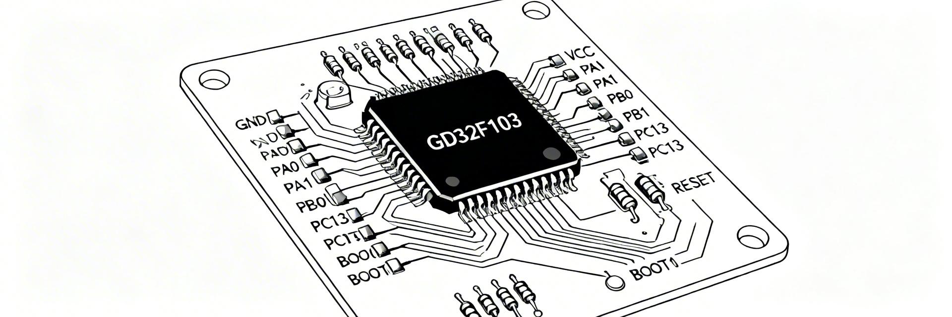
Pinout Breakdown & Functional Groups
Pin Grouping Strategy
Logical grouping simplifies layout. Separate power pins (VDD/VSS), analog reference (VREF), dedicated grounds, and many AF-capable pins (Alternate Function). Mapping these first ensures a cleaner GD32F103VBT6 pinout diagram and more stable signal integrity.
AF Remapping Strategy
AF conflicts are common in high-pin-count MCUs. Multiple peripherals share resources; remapping resolves contention. Prioritize power and clock pins, then critical communications like CAN or USB. Document chosen AF assignments early to avoid firmware surprises.
Electrical Characteristics & Safe Operating Limits
Power Rails & Sequencing
Verify rails and sequencing to protect silicon. Check VDD, VDDIO, and VBAT ranges as they differ by variant. Implement decoupling close to VDD pins and follow supply sequencing guidance to validate brown-out and reset behavior during bring-up.
IO Drive & Thermal Mitigation
GPIO drive current, ADC source impedance, and power dissipation affect reliability. Use series resistors for protection, size thermal vias for heat mitigation, and derate performance when many high-drive pins are active concurrently.
Performance Benchmarks & Throughput Tests
CPU & Memory Performance
Run tight-loop integer benchmarks like Dhrystone or CoreMark. Measure cycles per byte for memory operations and vary flash wait-states to quantify latency impact. Record timers and instruction per second for fine-tuning.
Peripheral Throughput
Expose bottlenecks caused by clocking and DMA contention. Log max sustainable throughput for SPI, UART, and USB. Compare DMA vs interrupt-driven modes; DMA usually increases sustained throughput significantly.
Real-world Case: Integration Examples
Example A — High-IO industrial controller
High-IO designs exploit many ADC/timer/UART resources. Reserve ADC pins for sensors, assign separate UART/SPI channels for modems, and plan CAN or RS485 transceivers. Validate isolation and EMC during prototype validation with a concrete checklist.
Example B — USB-enabled data logger with SD card
USB plus removable storage needs careful interface control. Reserve dedicated pins for USB D+/D-, ensure proper HSE oscillator placement, and implement caching to avoid data loss under latency during hot-plug scenarios.
Design & Deployment Checklist
PCB Layout Best Practices
- • Decoupling caps adjacent to VDD pins.
- • Continuous ground plane under high-speed traces.
- • Length-match critical SPI/USB lines.
Firmware Bring-up Checklist
- • Verify boot pin states and NRST.
- • Configure flash wait-states and clock tree.
- • Perform stress tests for thermal/IO limits.
Summary
- > The GD32F103VBT6 offers a high-pin-count mid-range Cortex-M3 solution; confirm specific specs and pin functions against the datasheet and prioritize pin mapping for I/O-heavy designs.
- > Create a labeled pinout mapping early, isolate analog pins, and plan AF remapping to avoid conflicts; validate power sequencing during prototype bring-up.
- > Run concise CPU and peripheral benchmarks—measure flash wait-state impact and DMA vs interrupt throughput to guide firmware tuning.
FAQ
What are the key GD32F103VBT6 pinout considerations for PCB layout?
Which GD32F103VBT6 specs most affect peripheral throughput?
How should engineers validate GD32F103VBT6 electrical limits during bring-up?
