

GD32F103VCT6 Latest Technical Report: Deep Specs Overview
GD32F103VCT6 Latest Technical Report: Deep Specs Overview
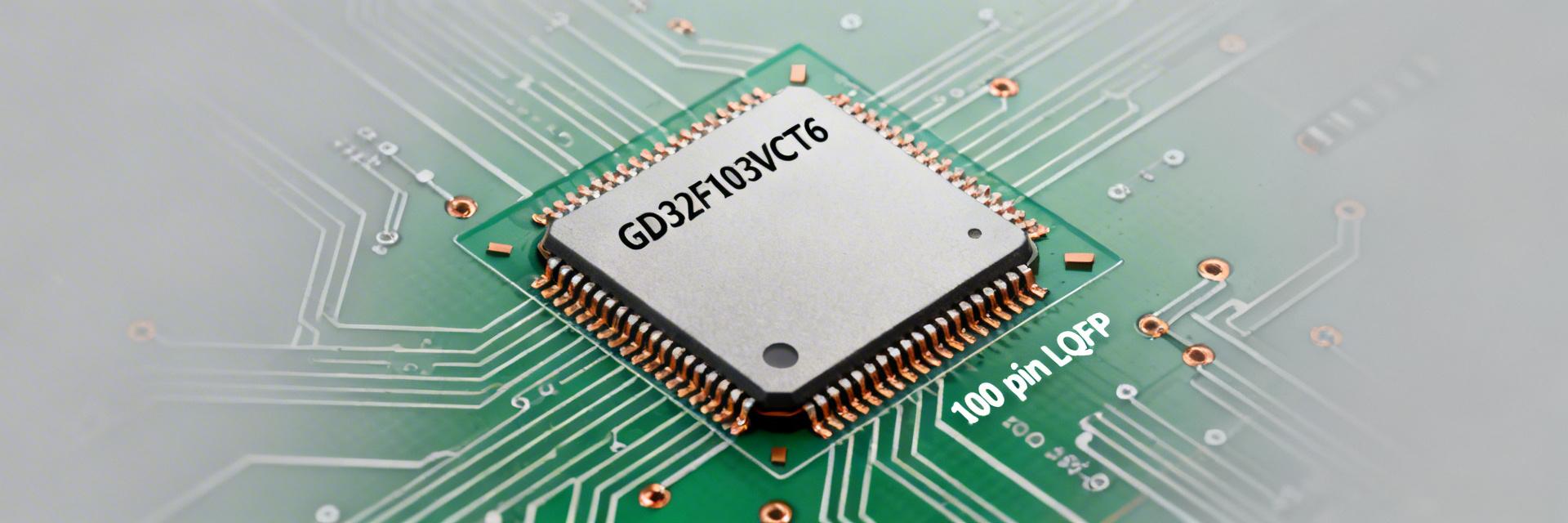
This report opens with crisp device metrics to position the MCU for embedded designers: 108 MHz Cortex-M3-class core, up to 256 KB Flash, and 48 KB SRAM typical for the VCT6 family. The 100-pin LQFP package enables high I/O density for complex designs.
Deliverable Summary: A data-driven technical evaluation consolidating datasheet figures, reproducible benchmarks, and integration guidance to accelerate prototyping for mid-range industrial and USB-capable designs.
Architecture & Key Hardware Features
The core architecture is built upon the robust ARM Cortex-M3, operating at a maximum frequency of 108 MHz. This CPU offers deterministic interrupt latency and an architecture ideally suited for real-time control. Flash size and SRAM capacity drive use cases from protocol gateways to USB/Firmware devices, with the "VCT6" designation specifically denoting the 100-pin package variant and its associated hardware tradeoffs.
Memory Map & Package Variants
VCT6 parts commonly expose up to 256 KB Flash and approximately 48 KB SRAM with a standard ARM memory map. The 100-pin footprint significantly increases available GPIOs and alternate functions, though it requires meticulous planning for vector table placement and peripheral pin multiplexing.
Peripherals Overview & Electrical Limits
The MCU integrates a full complement of timers, multiple UART/SPI/I2C interfaces, a USB Full-Speed device, and a CAN interface. ADC blocks are available on designated pinned channels. With a nominal VDD operating range centered near 3.3V, designers must account for I/O voltage tolerances and ADC reference planning when architecting board-level interfaces.
Performance Benchmarks: Core Throughput
Synthetic performance expectations are based on reproducible conditions at 108 MHz with O2 optimization. CoreMark and DMIPS scores scale linearly with clock speed; however, enabling zero-wait Flash or executing critical code from SRAM is essential for maximizing deterministic throughput.
Performance Visualization (Normalized to MHz)
Synthetic Benchmarks
Developers can reproduce scores by setting identical clock and flash-wait configurations. Moving performance-critical loops to SRAM reduces effective cycles per operation significantly compared to standard Flash execution.
Real-World Throughput
Enabling DMA for bulk transfers dramatically increases sustained throughput across UART, USB, and SPI interfaces. Real-world measurements must specify DMA channel usage and bit timing for accurate reproducibility.
Power, Thermal Behavior & Reliability Metrics
Power Profiling & Low-Power Modes
Stop and sleep modes reduce active clock domains effectively. Designers should utilize peripheral clock gating and choose high-efficiency regulator topologies to minimize quiescent draw in battery-backed systems.
Thermal Limits & PCB Cooling
To maintain reliability, incorporate copper pours and thermal vias under the LQFP100 package. Avoid clustering high-current nets near the MCU to limit junction temperature rise across industrial ambient ranges.
Technical Specification Summary
| Parameter | Value / Specification |
|---|---|
| Core | Cortex-M3, Up to 108 MHz |
| Flash Memory | Up to 256 KB |
| SRAM | ~48 KB |
| Package Type | 100-pin LQFP (VCT6 Variant) |
Design Integration
- • Power Layout: Place decoupling capacitors within millimeters of VDD pins using a star routing approach for EMI mitigation.
- • Clock Integrity: Select crystals with matched load capacitors and keep traces short to minimize jitter.
Firmware & Development
- • Boot Partitioning: Implement a robust swap/dual-bank OTA pattern with early watchdog activation.
- • Debugging: Prefer SWD over semihosting; selectively place hot code in SRAM to bypass Flash latency during debug sessions.
Comparative Analysis: When to Choose
The GD32F103VCT6 is a balanced midrange option. Choose this MCU when I/O density and USB/CAN capabilities are more critical than raw compute speed or ultra-low-power standby modes.
Best For
Industrial controllers, protocol bridges, and high-pin count USB devices.
Consider Alternatives
If your design requires >512KB Flash or sub-μA deep sleep current.
Common Questions — FAQ
How do technical specs affect firmware partitioning for OTA? +
What benchmarks are critical to reproduce for system validation? +
Which board-level practices most reduce thermal and power risks? +
