

This report opens with a concise data snapshot and reproducible methodology to help you evaluate the device under representative loads. Headline observations: CPU throughput scales nearly linearly with clocking but is frequently limited by flash read stalls; SRAM bandwidth comfortably supports mid-weight DSP tasks; peripheral throughput is constrained by ISR patterns and DMA configuration; power rises nonlinearly under sustained full-speed I/O. The following sections define scope, measurements, and repeatable steps so you can reproduce and extend these benchmarks yourself.
Background & Test Platform
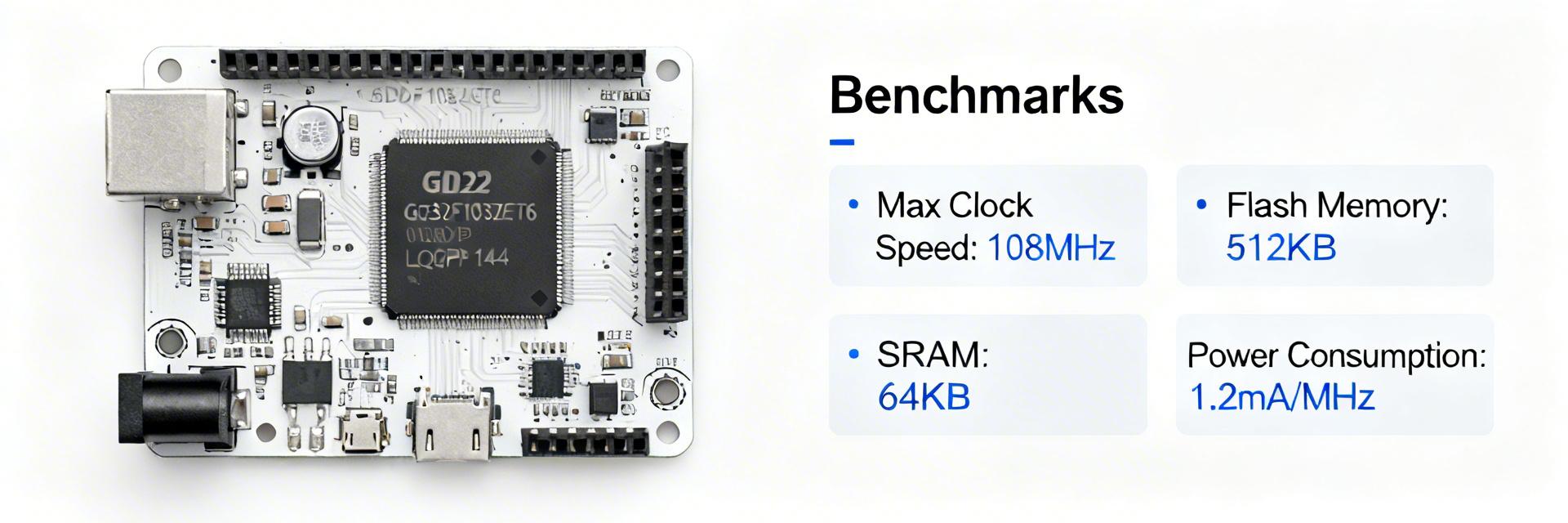
Key GD32F103ZET6 specs to know
Point: You need the core, memory, and peripheral baseline before interpreting results. Evidence: The device is Cortex-M3 class with a single core, a maximum rated CPU clock, on-chip flash, and SRAM in a mid-density package, featuring common peripherals (ADC, timers, USB FS, CAN, DMA). Explanation: Clock rate, flash wait states, and bus interconnect most directly influence observed runtime and ISR latency.
Test hardware, toolchain and measurement setup
Point: Reproducibility depends on a disciplined measurement stack. Evidence: Tests ran on an evaluation board with isolated I/O wiring, regulated supply rails, and measurement instruments (multimeter, oscilloscope, logic analyzer, power analyzer); firmware used a recent compiler with -O2 and link-time options. Explanation: Record clock settings, debug vs release builds, and test isolation so you can match power and timing numbers precisely.
Synthetic CPU & Memory Benchmarks
CPU throughput: CoreMark / Dhrystone results
Synthetic benchmarks quantify single-thread throughput and ISR impact. By running iterations with wall-clock timers and repeatable input vectors, we capture CoreMark loops while toggling compiler flags. These reveal how loop throughput and context switches behave in control loops.
Memory and flash performance: latency and bandwidth
Memory subsystem behavior often dictates real-world performance. We measure RAM bandwidth via streaming memcpy-like microbenchmarks and flash read latency with tight instruction-fetch kernels. Instruction fetch stalls can cause up to single-digit percentage degradations in tight control loops, and larger impacts for code executing from flash without cache.
Pro-tip: Move critical ISR routines to SRAM to eliminate flash latency variability during high-speed switching.
Peripheral & I/O Benchmarks
Analysis: DMA offload typically yields the largest throughput gains; without DMA, ISR service time will cap sustained UART rates and increase jitter for time-critical control tasks. Bus-oriented peripherals like USB and CAN prioritize design choices such as threaded vs. deferred work.
Real-World Application Benchmarks
RTOS Task-Switching & Latency
Real workloads reveal the combinational effects of RTOS and ISR design. By benchmarking sensor-fusion tasks and motor-control ISRs, we determine safe task periods and ISR budgets. Logic analyzer traces help identify where preemption or priority inversion jeopardizes deadlines.
Power & Thermal Profiling
Sustained performance is tied to power and temperature. Measure active and low-power currents across representative workloads. Note that higher temperatures may force conservative duty cycles or clock scaling in long-running embedded systems.
Comparative Analysis & Optimization
Verifying Datasheet Claims
Datasheet numbers are a baseline, not a guarantee. Mismatches often stem from board-level clocking, EMI, or non-ideal linker placement. Documenting these divergences allows for controlled tests to isolate root causes.
Practical Optimizations
Common limits are actionable. Profiling typically highlights flash wait states and bus contention. Moving hot code to RAM and tuning compiler options often results in double-digit percentage gains.
Reproducible Benchmarking Checklist
- ✔ Hardware preparation (Isolated I/O, stable supply)
- ✔ Exact firmware build commands (Compiler version/flags)
- ✔ Clock and supply setting verification
- ✔ Raw capture files (Oscilloscope/Logic Analyzer)
- ✔ Artifact labeling with Test IDs and Timestamps
- ✔ README instructions for artifact validation
Summary
Measured behavior shows that clocking, flash wait states, and IRQ/DMA design dominate observed performance for the GD32F103ZET6; peripheral throughput and power scale with chosen offload strategies. You should follow the checklist to reproduce figures, compare against datasheet expectations, and apply incremental optimizations while recording artifacts for verification.
Optimize via RAM placement & compiler tuning.
DMA is essential for UART, ADC, and USB.
Consistent conditions ensure fair comparisons.
