GD32F105RBT6 Technical Overview: Specs & Pinout Deep Dive

2026-02-06

Specs & Pinout Deep Dive for Professional Embedded Design

The GD32F105RBT6 is a compact ARM Cortex-M3 MCU targeted at connectivity and embedded control. Datasheet figures indicate a maximum core clock of 108 MHz with a 2.6–3.6 V supply window, making it suitable for battery-operated and regulated 3.3 V systems. This technical guide frames the device capability and sets expectations for electrical integration, pinout mapping, and production bring-up guidance for design engineers.

Core Clock: 108 MHz Supply: 2.6–3.6 V Core: ARM Cortex-M3

GD32F105RBT6 at a Glance — Core Specs Snapshot

GD32F105RBT6 Technical Overview Visualization

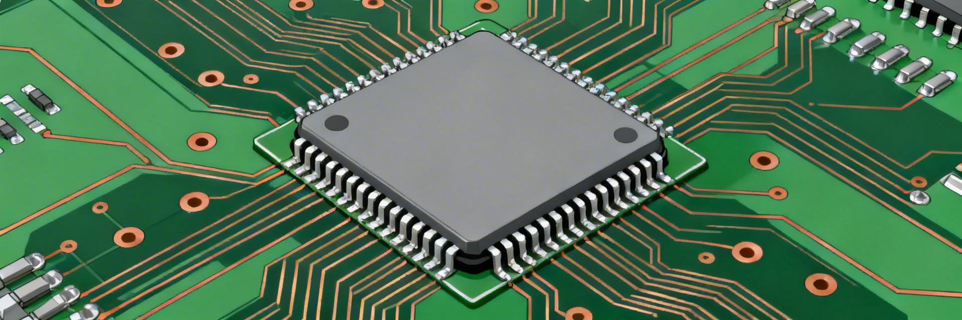
Figure 1: Silicon Architecture and Integration Flow

Key Silicon Characteristics

The MCU utilizes an ARM Cortex-M3 core, operating up to 108 MHz, and is housed in an LQFP64 package. Typical memory footprints for this family include 128 KB Flash and ~20 KB SRAM, positioning it as a mid-range MCU for robust control tasks. Designers should prioritize LQFP64 routing and thermal reliefs in PCB layout.

Performance Positioning

The mix of Cortex-M3 performance and peripheral density suits connectivity modules, sensor hubs, and real-time motor control. Its performance-to-power tradeoff favors systems requiring deterministic real-time behavior with modest code size, rather than high-end DSP intensive workloads.

Electrical Characteristics & Detailed Specs

Memory Resource Allocation

Flash: 128 KB
SRAM: 20 KB
Parameter Value / Range Design Guidance
Operating Voltage 2.6 V – 3.6 V Use low-noise 3.3V LDO
Core Frequency Max 108 MHz PLL-based clocking
I/O Type 5V Tolerant (most) Check datasheet for specific pins
Package LQFP64 10x10 mm footprint

Power, Clock and Reset Behavior

Designers should provide a low-noise 3.3 V regulator with 100–220 nF plus 10 µF decoupling at VDD pins. Correct sequencing of VDD and VSSA is essential. Choose crystal or ceramic resonator parameters compatible with the MCU's PLL limits to avoid lock failures during high-speed operation.

Boot and Programming Interfaces

Flash and RAM are mapped to standard Cortex-M regions. The part supports bootloader selection via dedicated BOOT pins. For debug, the device utilizes SWD/JTAG. Wire BOOT0/BOOT pins to test pads and expose an SWD 2x5 header for production firmware flashing and readout protection.

GD32F105RBT6 Pinout Deep Dive (LQFP64 Mapping)

Pin Summary & Signal Grouping

  • Digital I/O: High-speed routing area.
  • Analog (Vref/AVDD): Isolated quiet zone.
  • Special: NRST and BOOT selection pins.

Recommended PCB Routing

Apply ground pours with via stitching. Separate analog and digital domains where possible. Place local decoupling within 5 mm of VDD pins. Route high-speed signals away from noisy switching regulators to maintain ADC accuracy and minimize EMI.

On-Chip Peripherals: Timers, Comms, ADC, DMA

Timers & PWM

Multiple general-purpose timers support PWM channels and dead-time insertion. Crucial for motor control and LED dimming. Verify synchronization in firmware to prevent shoot-through.

Serial & Comms

Offers UART/USART, SPI, and I²C. Supports high-speed data transfer. Plan pin assignments early to avoid alternate-function conflicts on the LQFP64 footprint.

ADC & DMA

Pair ADC with DMA for low-CPU continuous acquisition. Use DMA circular mode for sensor streams to ensure deterministic performance without core intervention.

Design & Integration Checklist

Hardware Reliability

  • 0.1 µF and 1 µF ceramics at each VDD pin.
  • 10 µF bulk cap near the regulator.
  • Thermal vias under package ground plane.

Manufacturing & Test

  • 2x5 SWD pad footprint for debugging.
  • Exposed BOOT and NRST test points.
  • Labeled probe pads for UART diagnostic logs.

Troubleshooting & Firmware Tips

Common Integration Issues

Typical failures include missing clock start, brown-out resets, or incorrect boot selection. Debug flow: verify VDD rails, check NRST state, confirm crystal activity with a scope, and test BOOT pin levels.

Firmware Best Practices

Initialize the clock tree early. Enable peripheral clocks only when needed to save power. Set unused pins to analog or pulled states to reduce leakage. Implement a minimal watchdog and UART logging for first-power diagnostics.

Summary

  • GD32F105RBT6 offers a Cortex-M3 core up to 108 MHz with a 2.6–3.6 V domain; its specs favor deterministic control tasks with mid-range memory.
  • Key pinout considerations include dedicated power/analog pins and strategic grouping of high-speed signals on the LQFP64 footprint.
  • For production: prioritize strict decoupling, expose SWD/boot pads, and use ADC+DMA patterns to optimize CPU performance.

Frequently Asked Questions

What are the key specs for selecting the GD32F105RBT6? +
Consider the 108 MHz Cortex-M3 performance, 2.6–3.6 V supply requirement, and LQFP64 package. Match these to your system's memory needs, peripheral requirements, and power budget; ensure regulator and decoupling choices meet transient and brown-out thresholds to avoid erratic resets.
How should the GD32F105RBT6 pinout be handled for ADC accuracy? +
Route analog pins away from switching supplies, place AVDD and VREF decoupling close to the package, and keep analog traces short. Use separate analog ground pours if board real-estate allows, and avoid multiplexing noisy digital functions onto ADC input pins during precision sampling.
What are recommended first steps for firmware bring-up? +
Start with a minimal startup that configures clocks, enables a basic UART for logs, sets unused pins to safe states, and verifies flash/programming via SWD. Add ADC+DMA or a timer test next to confirm peripheral clocks and interrupt routing before loading complex application code.