

Typical SPI Interface Operating Frequency
*Design teams measure failed boots and corrupted reads tied to misrouted SCLK or incorrect CS polarity.
Background: GD25W515TIQ6 at a Glance
Product Role & Common Use Cases
The device is a serial NOR flash intended for code and data storage in constrained embedded systems. Designers typically choose SPI NOR for boot ROM, firmware store, and lookup tables because of its low pin count and simple protocol. Verify whether the application needs single-, dual-, or quad-I/O modes and ensure write/erase endurance meets the firmware strategy.
Package Types & Pin-Count Caveats
Pinout Map: Pin-by-Pin Breakdown
| Pin Category | Signal Name | Electrical Role & Requirements |
|---|---|---|
| Power | VCC, VSS/GND | Requires local decoupling (0.1 µF + 1 µF–4.7 µF). Place bypass within 1.5mm of the pin. |
| Control | CS#, SCLK | CS is active low; SCLK idles high/low based on CPOL. Keep control pins near host MCU. |
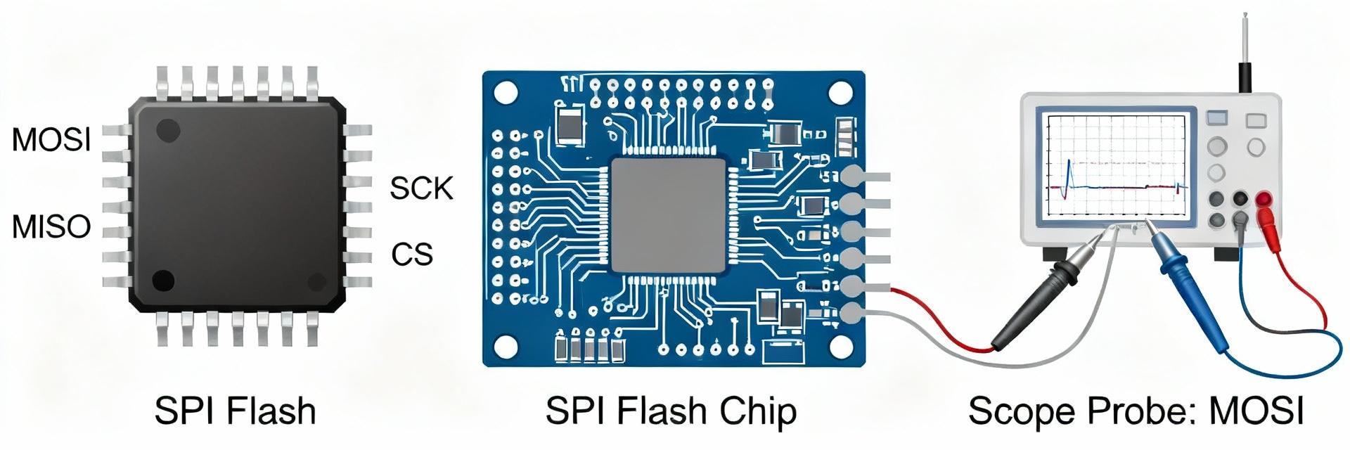
| Data I/O | SI (IO0), SO (IO1) | Standard MOSI/MISO. SI is host-driven; SO is device-driven. |
| Extended I/O | WP# (IO2), HOLD# (IO3) | Used in Quad-SPI mode. Add recommended pull-ups to disable protection when unused. |
SPI Signal Behavior & Mode Mapping
CPOL/CPHA Recommended Settings
The four SPI modes determine which clock edge latches data. If data appears offset by one bit, the host likely uses the wrong CPHA setting. Use a decision flow: capture CS and SCLK, note idle state (CPOL), then shift CPHA until reads match expected ID.
Setup/Hold & Drive Strength
Enable series resistors (22–33 Ω) on SCLK/MOSI to damp reflections. Start with a conservative clock (e.g., 25–33% of max) and increase speed only after waveform validation via oscilloscope.
Wiring Patterns & PCB Layout Best Practices
- ✔ Routing & Topology: Route short, direct traces between MCU and flash. Keep SCLK and CS away from noisy clock lines or switching regulators.
- ✔ Grounding Strategy: Use a solid ground plane and stitch vias for return paths. Ensure VCC is present before the host drives MOSI to prevent latch-up.
- ✔ Termination: Use 22–33 Ω source resistors for sub-inch traces to resolve ringing without complex impedance control.
Practical Debugging Checklist
Symptom-Driven Quick Checks
• Validate voltage rails with a multimeter.
• Confirm CS idles High (active-low logic).
• Verify physical continuity from MCU pad to Flash pin.
• Check pull-ups on WP/HOLD pins.
Instrument & Advanced Steps
• Record waveforms at 4× the clock rate.
• Look for tri-state conflicts on the MISO line.
• Decode the "Read ID" command via logic analyzer.
• Slow the clock to expose margin issues.
Summary
Mastering the GD25W515TIQ6 pinout and SPI signal behavior avoids common integration pitfalls and shortens time-to-working firmware. Teams that standardize decoupling, routing, and timing checks reduce bring-up iterations. Verify the package and datasheet before layout, wire power and ground with proper decoupling, and match SPI mode/timing. These steps accelerate the reliable integration of this SPI flash memory into any embedded product.
