
GD32A503 MCU Datasheet Deep Dive: Key Specs & Benchmarks

GD32A503 MCU Datasheet Deep Dive: Key Specs & Benchmarks

2026-02-09

GD32A503 MCU Datasheet Deep Dive: Key Specs & Benchmarks

The GD32A503 MCU targets the upper tier of Cortex-M33 automotive and industrial controllers with a 100 MHz core-class performance profile. This deep dive decodes technical specifications into concrete engineering actions for system tradeoffs and verification.

Performance Benchmarks at 100 MHz

CoreMark Score Range 250 – 320
DMIPS Performance 120 – 140

A Automotive & Embedded Design Positioning
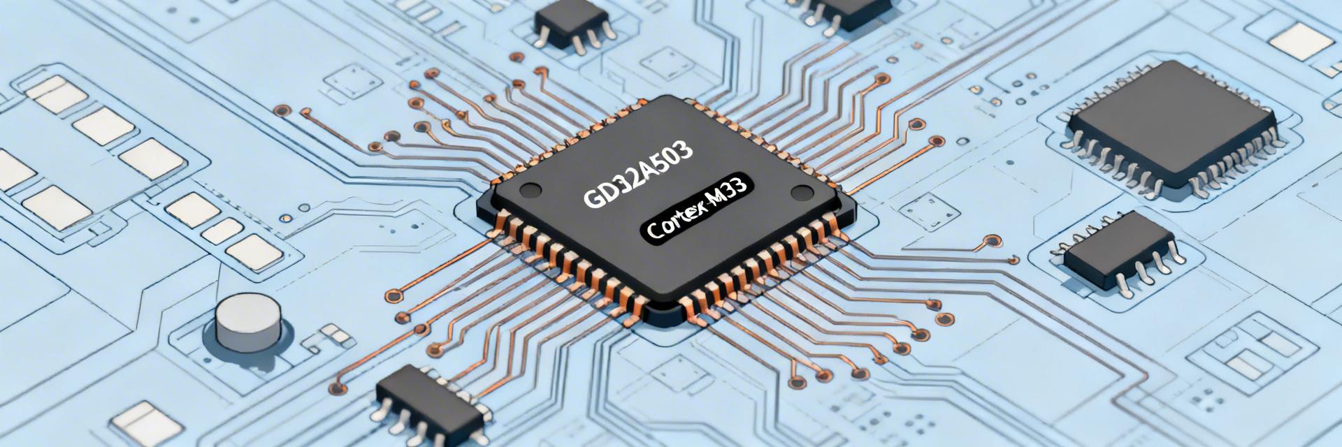
GD32A503 MCU Architecture Overview

Positioning and Intended Use Cases

The device is positioned for safety-adjacent automotive and industrial control, real-time motor control, and mid-range HMI tasks where deterministic timing and ISO/EMC margins matter. For GD32A503 MCU automotive use cases, prioritize bounded ISR latency, reliable peripheral offload, and power sequencing that meet vehicle electrical transients and extended temperature ranges typical of these product families.

Core Architecture at a Glance

Built around a 100 MHz Cortex-M33-class core, expected security partitions or TrustZone-like features and hardware accelerators reduce context switch overhead. Low interrupt latency and predictable preemption depend on NVIC implementation, cache/prefetch behavior, and whether FPU/crypto units exist — all critical for ISR cost, real-time scheduling, and hardware-assisted workloads.

Electrical & Clock Specifications

Supply and Operating Ranges

Parameter Recommended Range Critical Consideration
Supply Voltage 2.7V – 3.6V Absolute max margins exceed this; monitor transients.
Max Frequency 100 MHz Scale flash wait states above 60-80 MHz.
I/O Levels CMOS/TTL Compatible Check per-package current sink/source limits.

Clock Domains and PLL Behavior

Expect internal RC and external crystal options with PLL multiplication to the 100 MHz CPU domain; separate bus and peripheral dividers govern APB/AHB clocks. Size flash wait states conservatively at first (test at target voltage/temperature) and use bus dividers to ensure peripheral timing stability; verify flash latency tables in the datasheet when scaling above 60–80 MHz.

Memory & Execution

  • ◈ Flash/SRAM Layout: Plan linker regions for bootloader, application, and DMA buffers.
  • ◈ Optimization: Place latency-sensitive routines in zero-wait or cacheable regions.
  • ◈ DMA Efficiency: Align flash reads to avoid CPU stalls and maximize sequential fetches.

Peripheral Ecosystem

  • ◈ Connectivity: UART, SPI, I2C, and FDCAN for high-reliability networking.
  • ◈ Analog Blocks: 12-bit ADCs, DACs, and comparators for precise sensor conditioning.
  • ◈ Timers: Advanced PWM units and high-resolution timers for motor control.

Design Integration FAQ

What are the thermal and EMC considerations for layout?
Place decoupling close to VDD pins, use solid ground planes, and segregate noisy power rails. Thermally derate clock and I/O timing at high ambient; include thermal vias under high-power packages. For EMC, add common-mode filtering on high-speed lines.
How should real-world benchmarks be conducted?
Define scenarios like ADC sampling with DMA, FDCAN throughput, and PWM updates. Capture ISR entry/exit using GPIO toggles and a logic analyzer to measure latency and jitter compared against datasheet envelopes.
What are the typical cost vs. performance tradeoffs?
Choose package and memory trims based on required Flash/SRAM and I/O count. Prefer lower clock scaling for battery-constrained platforms and higher trims where sustained DMA throughput and processing power are dominant.

Summary for Engineers

Verify three key specs: Maximum CPU/Bus frequencies with wait states, supply/thermal derating, and DMA channel availability. Run CoreMark/DMIPS at target clocks and measure ISR latency via GPIO. Immediate action: set conservative wait states and lock a memory map separating bootloader from application logic.

100 MHz Core
Cortex-M33
Automotive Grade