GD32E103RBT6 Technical Report: Benchmarks & Key Specs

GD32E103RBT6 Technical Report: Benchmarks & Key Specs

2026-02-10

This technical report examines recent benchmark trends for Cortex-M4-class microcontrollers and explains why the GD32E103RBT6 warrants focused evaluation. Observed trends emphasize competitive integer throughput, balanced memory and peripheral mixes, and favorable active/sleep power profiles for mid-range embedded tasks.

The report scope covers key technical specifications, benchmark methodology and results, comparative use-cases, and actionable engineering recommendations designed for rapid validation and reliable deployment.

Structured for engineering teams, the report provides reproducible test checklists, normalized comparison templates, and pragmatic hardware and firmware checklists that accelerate time-to-proof. It targets designers evaluating mid-range MCUs for control loops, sensor fusion, motor control, and battery-powered telemetry nodes, offering measurable pass/fail thresholds and optimization tactics aligned with global engineering practices.

Background: Cortex-M4 Position & Target Applications

GD32E103RBT6 Technical Report: Benchmarks & Key Specs

Where this MCU fits in embedded design

Point: The Cortex-M4 family strikes a balance between deterministic control and signal-processing tasks. Evidence: M4 cores typically include DSP extensions and optional single-precision FPU, enabling efficient integer and floating-point math for control loops and filtering. Explanation: For real-time motor control, sensor fusion, and mid-complexity RTOS applications, M4-class performance allows higher control loop rates and lower interrupt latency than lower-tier cores.

Package, memory and power envelope

Point: Designers must confirm package, memory and supply constraints early. Evidence: Typical pin counts offer 48–100 pins, flash in the 64–128KB range, and SRAM in the 20–32KB region. Explanation: These bounds define peripheral availability, external memory options, and the thermal/power strategy for sustained high-frequency operation.

Parameter Typical Value Engineering Note
Package 64-pin LQFP Confirm I/O count vs required UART/SPI/PWM
Flash
128 KB
Plan bootloader & OTA partitioning
RAM
32 KB
Reserve for RTOS stacks and DMA buffers
Vcc 2.6–3.6 V Check ADC reference and GPIO tolerance
I/O count ~48 usable GPIO Map high-speed pins early

GD32E103RBT6: Key Technical Specifications (Detailed)

These technical specifications summarize core, clocks, memory architecture, and peripheral capabilities to inform benchmark expectations and hardware design trade-offs.

Core, Clocks and Memory Architecture

Point: Core revision and clocking directly affect integer throughput and real-time determinism. Evidence: The device uses a Cortex-M4-class core with a nominal top CPU frequency in the 108–120 MHz class. Explanation: Designers should tune flash wait-states and bus prescalers; memory map includes internal flash with boot and option bytes plus embedded SRAM.

Spec Item Nominal Value Engineering Note
Core Cortex-M4-class Verify FPU/DSP support for math-heavy workloads
Max CPU freq ~108 MHz Balance performance vs power and flash WS
Peripherals ADC/DAC/Timers Validate input ranges and DMA prioritization

GD32E103RBT6 Benchmarks & Test Methodology

Benchmark Suite & Conditions

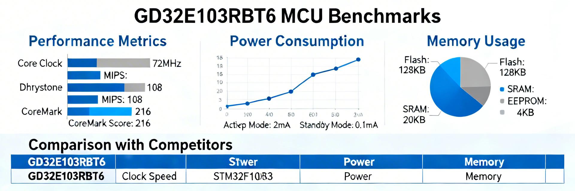
Point: Reproducible benchmarks require defined toolchains and measurement conditions. Evidence: Recommended suite includes CoreMark, Dhrystone (DMIPS/MHz), integer/FP microbenchmarks, and memory throughput. Explanation: Use a consistent compiler with explicit optimization flags (e.g., -O3), fixed clock configuration, and calibrated power meters.

Key Metrics & Presentation

Point: Select metrics that map directly to system requirements. Evidence: Report CoreMark score, DMIPS/MHz, and memory read/write MB/s. Explanation: Present results with bar charts for core scores and tables for power versus frequency to make results actionable.

Hardware Design Checklist

  • ✔ Close decoupling at Vcc pins
  • ✔ Dedicated analog ground for ADC inputs
  • ✔ Careful crystal routing and EMI filtering
  • ✔ Implement brown-out and reset settings

Firmware Tuning Checklist

  • ⚙ Use architecture-specific compiler flags
  • ⚙ Align critical code to faster memory regions
  • ⚙ Enable hardware FPU/DSP for math loads
  • ⚙ Employ clock gating for unused peripherals

Summary

  • The GD32E103RBT6 delivers a balanced mid-range Cortex-M4-class combination of core throughput, integrated peripherals, and manageable power for control and sensing applications.
  • Adopt the provided test checklist and normalization templates to ensure fair comparisons and identify flash wait-state and DMA bottlenecks early in development.
  • Follow the hardware and firmware checklists—decoupling, ADC front-end, compiler flags, and power gating—to reduce iteration cycles and risk when scaling to production.

Frequently Asked Questions

What performance benchmarks should I run for GD32E103RBT6? +
Run CoreMark and Dhrystone for CPU-level comparison, microbenchmarks for integer/FP kernels used by your firmware, memory throughput tests for DMA, and ADC sampling stress tests. Include power measurements at each frequency and load case to correlate performance with energy consumption.
How do I optimize power for battery designs using this MCU? +
Use peripheral and clock gating to disable unused blocks, select lowest viable clock for idle states, and use DMA to keep CPU in low-power modes. Choose an efficient regulator (buck for wide input ranges), configure brown-out/reset properly, and verify sleep/wake latencies against your sampling windows.
What are common pitfalls when benchmarking and validating this class of MCU? +
Common pitfalls include inconsistent compiler flags, unreported flash wait-states that throttle throughput at high clocks, insufficient thermal control when measuring power, and ignoring ISR-induced jitter. Mitigate these by automating runs and documenting toolchain settings.