

GD32E103TBU6 Datasheet Deep-Dive & QFN-36 Layout Insights
As compact Cortex-M4-class MCUs power modern industrial and consumer electronics, precise layout choices determine first-pass hardware success.
Insight: Targeted datasheet interpretation and precise QFN-36 land-pattern choices are critical. This guide provides a data-focused walkthrough, highlighting the tables and verifiable layout actions that hardware engineers, PCB designers, and firmware leads can apply immediately.
Background & Package Overview
Device Family Position & Key Specs
Start with the device summary and feature table to map system constraints quickly. The GD32E103TBU6 datasheet lists the CPU core, max clock, Flash, and RAM sizes, which are essential for determining regulator choices and memory budgets.
QFN-36 Mechanical Footprint and Pinout Summary
Extract the mechanical drawing to define your land-pattern and QFN-36 pinout. Key dimensions include the package outline, pad count, exposed pad size, and pin orientation. Pin numbering in the datasheet table identifies critical boot, reset, and SWD pins.
Datasheet Deep-Dive: Electrical & Thermal Data
Absolute Maximums & Operating Conditions
Distinguish between absolute maximums and recommended conditions to prevent component overstress. Below is a normalized view of the operating parameters:
| Parameter | Min Value | Max Value | Unit |
|---|---|---|---|
| Supply Voltage (VDD) | 2.6 | 3.6 | V |
| I/O Input Voltage | -0.3 | VDD + 0.3 | V |
| Operating Temperature | -40 | 85 / 105 | °C |
Thermal Resistance & Power Visualization
Convert θJA/θJC guidance into practical PCB power budgets. Estimate junction temperature with Tj = Ta + P · θJA.
Pin Functions & Peripheral Mappings
Pin Multiplexing Strategy
- ::marker Reserve Power, Reset, and Boot pins first.
- ::marker Prioritize high-speed interfaces (SPI/I2C/USART).
- ::marker Lock SWD pins during layout review.
Decoupling Requirements
Place 0.1µF ceramic caps at each VDD pin. Use a 4.7–10µF bulk capacitor near the regulator. Route shortest possible traces to minimize loop inductance and EMI.
QFN-36 PCB Layout Insights
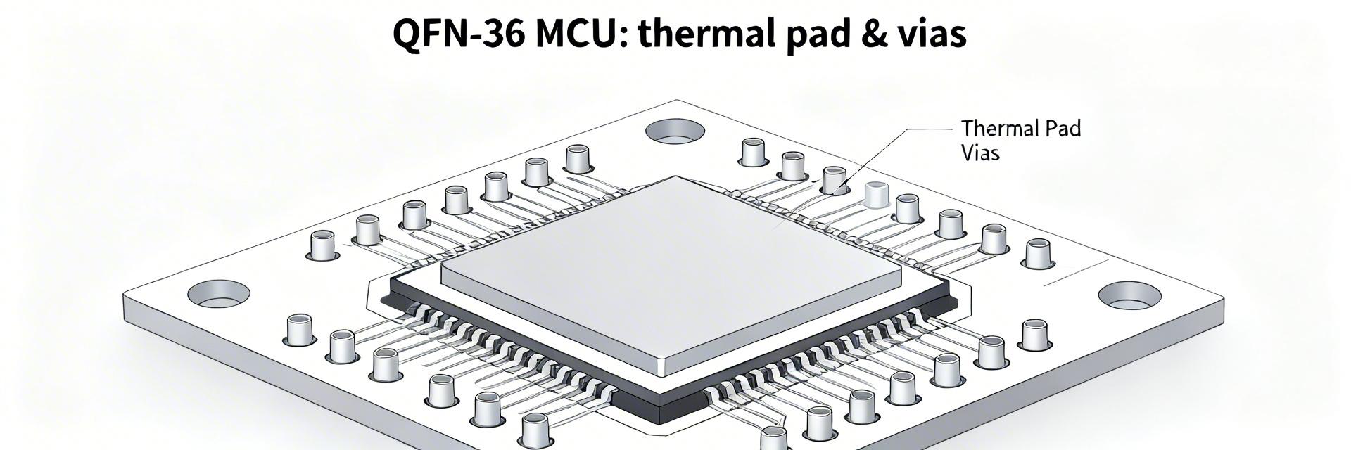
Thermal Pad & Solder Mask Design
Translate mechanical tolerances into a conservative land pattern. Create a single exposed pad with segmented solder paste apertures (30–40% coverage) to control solder volume and prevent voiding or component "floating."
Implementation Checklist:
Validation & Troubleshooting
Common Pitfalls
- Missing thermal vias in the exposed pad.
- Inadequate decoupling capacitance.
- Routing high-speed nets under the MCU core.
Bring-up Checklist
- Verify VDD/VREF voltage and ripple.
- Check Reset and Clock stability.
- Confirm SWD connectivity and die temp.
Summary
Start with the device summary and power/thermal tables. Enforce conservative land-pattern and thermal-via design for QFN-36 assemblies. The top layout actions are correct exposed pad design, an adequate thermal via grid, and precise decoupling placement.
Frequently Asked Questions
What key datasheet tables should I capture for GD32E103TBU6 design?
How many thermal vias are recommended for a QFN-36 exposed pad?
Which decoupling caps and placement pattern are best for this MCU?
