

GD32E230K8T6 Datasheet Deep Dive: Key Specs & Metrics
The GD32E230K8T6 features a 72 MHz Cortex-M23 core, 64 KB Flash, and 8 KB SRAM. Operating within a 1.8–3.6 V window in an LQFP-32 footprint, these specifications define the device's power envelope, memory capacity, and PCB constraints for modern embedded designs.
Product Positioning & Common Use Cases
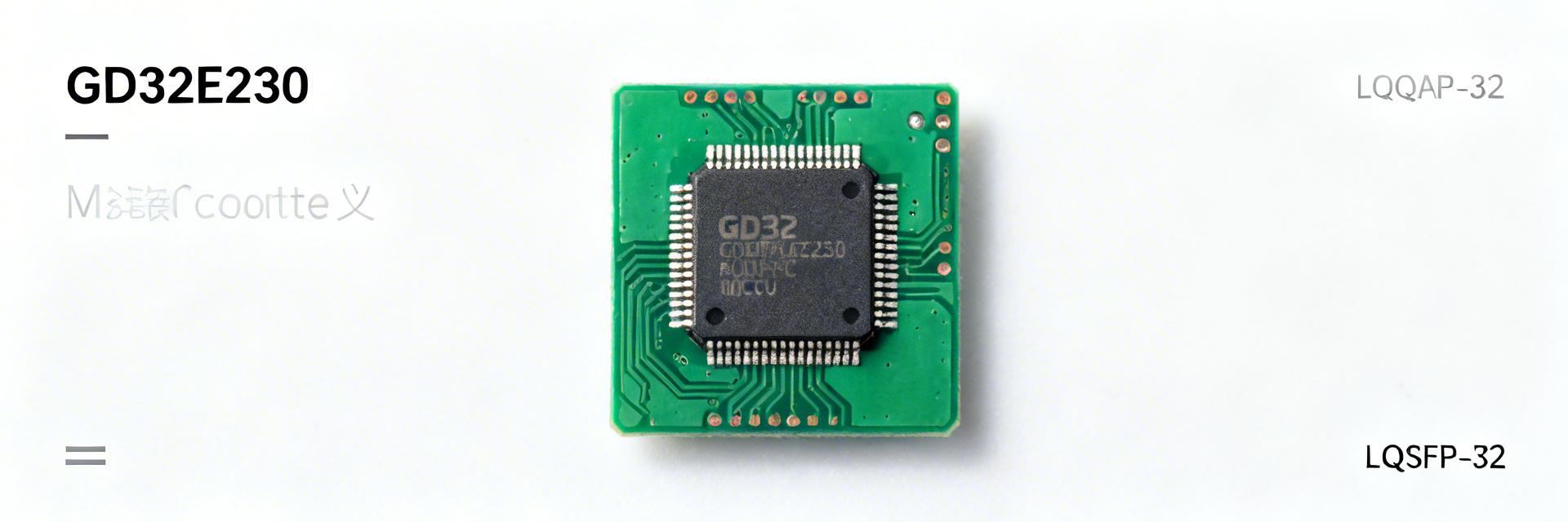
Positioned as an entry-level 32-bit MCU, the GD32E230K8T6 targets cost-sensitive, low-to-moderate compute tasks where a compact package and modest memory are sufficient. Its Cortex-M23 core and streamlined RAM/Flash resources make it highly attractive for single-purpose products and battery-operated nodes, rather than feature-rich, multitasking systems requiring extensive memory or complex OS support.
Target Application Profiles
Ideal for low-power sensor nodes, simple control panels, and single-function peripherals. The 8 KB SRAM constraints require event-driven firmware and small protocol implementations, often offloading heavy processing to gateways.
Board & Package Considerations
The LQFP-32 package balances cost and I/O density. Engineers should budget pins for power, debugging, and analog functions. For minimal BOM, utilize internal oscillators and eliminate unnecessary external peripherals.
Core, Memory, Clock, and Voltage Analysis
Utilizing an Arm Cortex-M23 core running at up to 72 MHz, the device's 64 KB Flash limits large bootloaders, while the 8 KB SRAM necessitates aggressive code-size optimization and linker garbage collection.
Performance & Analog/Digital Peripherals
Timers & Communication
Features 16-bit timers supporting PWM and input capture. SPI rates can reach 8–24 MHz depending on layout, while UART links benefit from DMA and hardware flow control to maintain stability under high bus contention.
ADC & Analog Performance
The 12-bit ADC provides adequate resolution but requires isolated VDDA and RC filtering. It is recommended to implement calibration routines at startup to maximize the Effective Number of Bits (ENOB).
Design Case Studies
Case A: Low-Power Wireless Sensor Node
Using ADC for sensing and SPI for radio control. Optimized for low μA current via aggressive sleep duty cycling. Firmware footprint: ~25 KB Flash / 3 KB SRAM.
Case B: Simple HMI / Control Panel
UART/I2C for display and input. Flash contains UI assets; images must be minimal or compressed. SRAM is prioritized for stack and display streaming buffers.
Production Checklist & Testing
- ✔ Pre-silicon: Include 0.1 μF + 1 μF decoupling per VDD; verify dedicated VDDA/VSSA nets.
- ✔ Clocking: Configure PLL and flash latency per datasheet when scaling to 72 MHz.
- ✔ Validation: Measure power in all modes; verify ADC linearity and UART loopback integrity.
Common Questions & Answers
Can the GD32E230K8T6 run an RTOS given the 8 KB SRAM? +
What are practical ADC accuracy expectations? +
How should developers verify low-power behavior? +
