

GD32E230K8U6 MCU: Full Specs, Pinout & Price Guide
As designers push for higher efficiency at lower BOM cost, the GD32E230K8U6 emerges as a compact 32-bit option with a Cortex-M23 core, up to 72 MHz, 64 KB flash, and a focused peripheral set tailored for low-power embedded nodes.
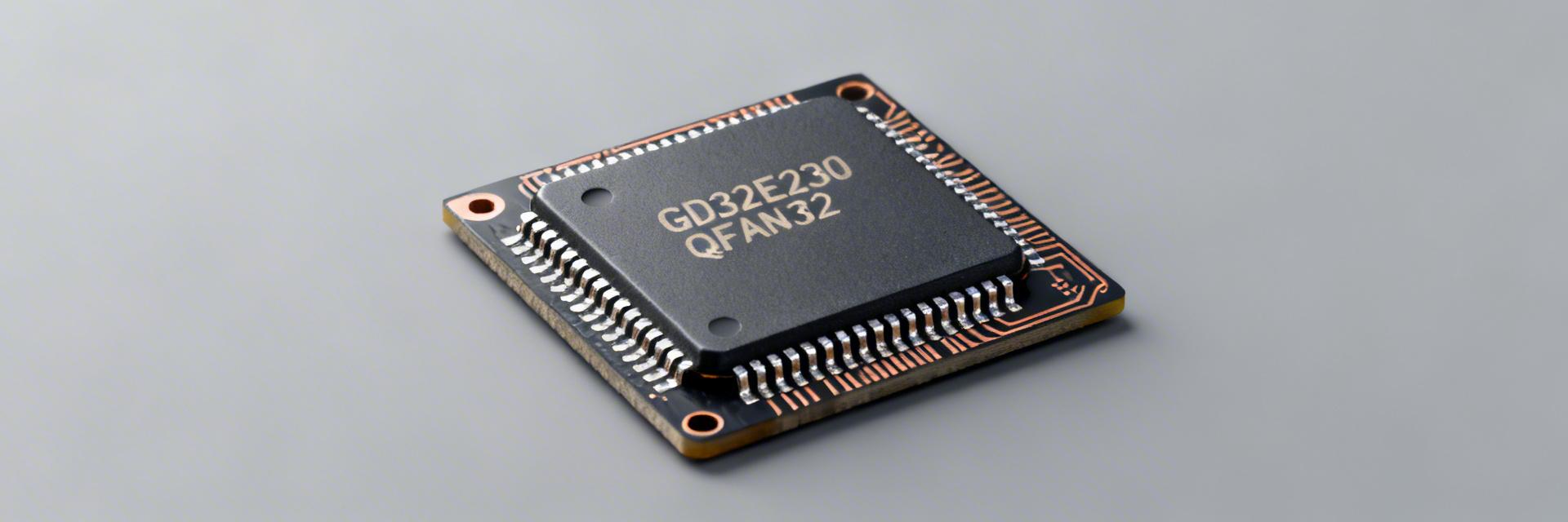
Overview: GD32E230K8U6 at a Glance
This article delivers full specs, clear pinout guidance, PCB/integration tips, and realistic price and sourcing advice to accelerate early design decisions. Readers will get an at-a-glance overview, detailed technical tables, and programming recipes to inform prototyping.
Key Selling Points
The device is a cost-focused 32-bit MCU built around an Arm Cortex-M23 core at up to 72 MHz. Its balance of compute and low active power targets battery-powered instruments and wearables.
- CPU: Cortex-M23, up to 72 MHz
- Flash/SRAM: 64 KB / 8–16 KB
- Voltage Range: 2.0–3.6 V
- Package: QFN32 (Optimal thermal)
Typical Use Cases
Fits cost-sensitive, low-power products where feature sets emphasize ADCs and basic serial ports over high-end DSP capabilities.
- Battery Sensor Nodes — Low active current.
- Wearables — Compact package and sleep modes.
- Simple Motor Control — Dedicated PWM timers.
Full Technical Specifications
Core, Memory, and Performance
The core and memory set the performance envelope. Cortex-M23 at 72 MHz with 64 KB flash gives deterministic real-time performance for control loops.
Peripherals, ADC/DAC, and Comms
Peripherals favor analog and basic serial communications. Use pin remapping carefully to preserve ADC accuracy and manage shared resources.
- ADC: 12-bit, multi-channel multiplexing.
- Comms: UART, SPI, I2C available.
- DMA: Limited — plan CPU cycles.
- Timers: PWM for basic control tasks.
Pinout, Package Options and PCB Integration
Pinout Map and Signal Descriptions
Map power, analog, and comms pins first. Reserve boot and reset pins to simplify layout and troubleshooting.
| Pin | Primary Function | Integration Notes |
|---|---|---|
| VDD | Power Supply | Decouple per supply pin |
| VREF | Analog Ref | Quiet, short trace route |
| PAx/PBx | GPIO/ADC/Comm | Multiplexed—check remap |
PCB Best Practices
- 1. Place decoupling within 1–2 mm.
- 2. Stitch ground vias to thermal pad.
- 3. Keep ADC traces away from noise.
- 4. Solid ground plane mandatory.
Development and Example Configurations
Typical Flashing Sequence
Implement a 4-pin header footprint (VDD, GND, SWCLK, SWDIO) for easy debug access.
Pseudocode Recipe: Configure ADC channel → Start conversion → Poll/Interrupt → Read result → Apply calibration offset.
Price Range and Sourcing Strategy
Sourcing Checklist
- ✓ Datasheet Revision Check
- ✓ Lot Code Verification
- ✓ Sample Traceability
- ✓ Lead-time Agreement
- ✓ Packaging Confirmation
- ✓ Functional Bench Test
Key Summary
Common Questions and Answers
