

GD32E501REL7 datasheet: quick pinout & key specs guide
This professional guide extracts critical data from the GD32E501REL7 datasheet to provide an engineer-ready pinout and key technical specifications. The GD32E5 family supports single-supply operation (2.7–3.6 V) and high-speed processing up to ~200 MHz.
Background — Device Architecture and Positioning
Core Device Overview
The GD32E501REL7 is a premium member of the Cortex-M33 class microcontroller family, specifically engineered for mid-range embedded systems. While higher-end GD32E5xx parts push the performance ceiling, the GD32E501 series maintains a balanced performance-to-power ratio. It is essential to treat this as a high-precision M-class MCU with integrated memory and I/O tiers optimized for consistent timing budgets.
Package Variants & Target Applications
Offered in various footprints like QFN and LQFP, many variants feature exposed pads for superior thermal relief. Recommended application domains include:
- ▶ High-Precision Motor Control
- ▶ Industrial Automation Units
- ▶ High-Density IoT Endpoints
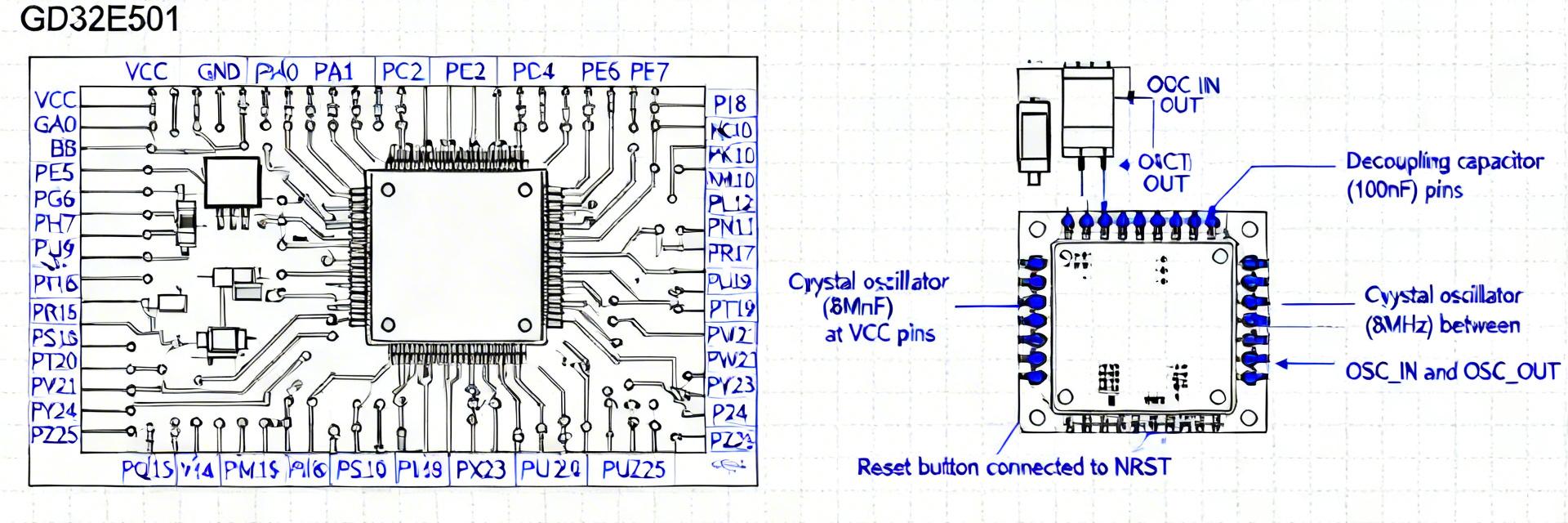
| Package Type | Pin Count | Context |
|---|---|---|
| QFN / LQFP | SKU Dependent | IoT & Motor Control |
Data Analysis — Electrical & Performance Specs
System Performance Visualization
| Parameter | Design Target (Required Verification) |
|---|---|
| Operating Voltage | 2.7–3.6 V (Single Supply Range) |
| Core/System Clock | Device-specific (~100 MHz for GD32E501 class) |
| Flash / SRAM | Variant-dependent densities |
| Security / MPU | Integrated MPU and Secure Boot Blocks |
CRITICAL WARNING:
Always verify absolute maximum ratings and thermal derating in the official datasheet. Decoupling capacitors (0.1 μF + 1 μF) must be placed as close as possible to VDD pins.
Method Guide — Pinout, Mapping and Common Signals
Primary Pin Assignment
| Symbol | Function | Notes |
|---|---|---|
| VDD | Power Supply | Local Decoupling |
| VSS | Ground | Common Plane |
| NRST | System Reset | Ext. Pull-up Req. |
Multiplexing & Boot
Identify pins affecting boot modes (Boot0/Boot1) and SWD/NJTRST debug interfaces. Utilize the Alternate Function (AF) table to resolve pin conflicts during schematic design.
1. Power/GND Rails
2. Crystal/Clock Sources
3. Boot & Debug (SWD)
4. High-speed Peripherals
Case Examples — Application Configuration FAQ
How do I implement a minimal power-and-programming setup?
Provide stable VDD and VSS connections with 0.1 μF decoupling per pin. Route the NRST line with a 10 kΩ pull-up resistor. Expose SWDIO and SWCLK to a standard header for programming. If your design requires precise timing, integrate a 32.768 kHz crystal following strictly defined layout guidelines to minimize parasitic capacitance.
What are the common peripheral mappings for this MCU?
- UART Console: Usually mapped to USART1 pins for debugging.
- I2C Sensors: Typically on PB pins using open-drain routing with external pull-ups.
- SPI Flash: Dedicated SPI pins with high-speed layout considerations for Chip Select (CS) routing.
Action Checklist — Design Verification
PCB & Schematic
- ✅ All VDD/VSS pins routed and decoupled
- ✅ Exposed pads connected via thermal vias
- ✅ High-speed trace rules for clock lines
- ✅ NRST and Boot pins easily accessible
Firmware & Bring-up
- ✅ Connect SWD and verify Device ID
- ✅ Disable unused internal pull-ups
- ✅ Calibrate system clock sources
- ✅ Test flash read/write connectivity
