

GD32F103RBT6 Specification Deep-Dive: Benchmarks & Limits
GD32F103RBT6 Specification Deep-Dive: Benchmarks & Limits
Translating datasheet figures into realistic performance expectations and actionable design trade-offs for system engineers.
Product Positioning & Use Cases
Point: Targets cost-sensitive embedded control and connectivity tasks.
Evidence: Features Cortex-M3 performance, USB FS, and CAN 2.0B peripherals.
Explanation: Ideal for general-purpose controls, USB/CAN nodes, and motor-control assistants where deterministic performance meets low system cost.
Package & Pinout Logistics
Point: LQFP64 package constraints require strategic routing.
Evidence: High-density I/O including ADC channels, Timers, and Communication ports.
Explanation: Maintain controlled impedance for USB/CAN traces and ensure robust decoupling near VDD/VSS pins to limit EMI.
Technical Specification Snapshot
Performance Benchmarks — Measured vs Spec
CPU Throughput (CoreMark Score)
Peripheral Throughput (DMA Enabled vs CPU Driven)
Thermal & Power Constraints
Sustained high-clock operation increases die temperature. At 108 MHz, power dissipation rises significantly. Monitor junction temperature and optimize PCB copper area for heat dissipation.
Timing & EMI Reliability
Worst-case bus contention can lead to missed deadlines. High-frequency edges on USB/CAN traces raise EMI risks. Implement brownout resets and watchdogs for robust production code.
Benchmarking Methodology
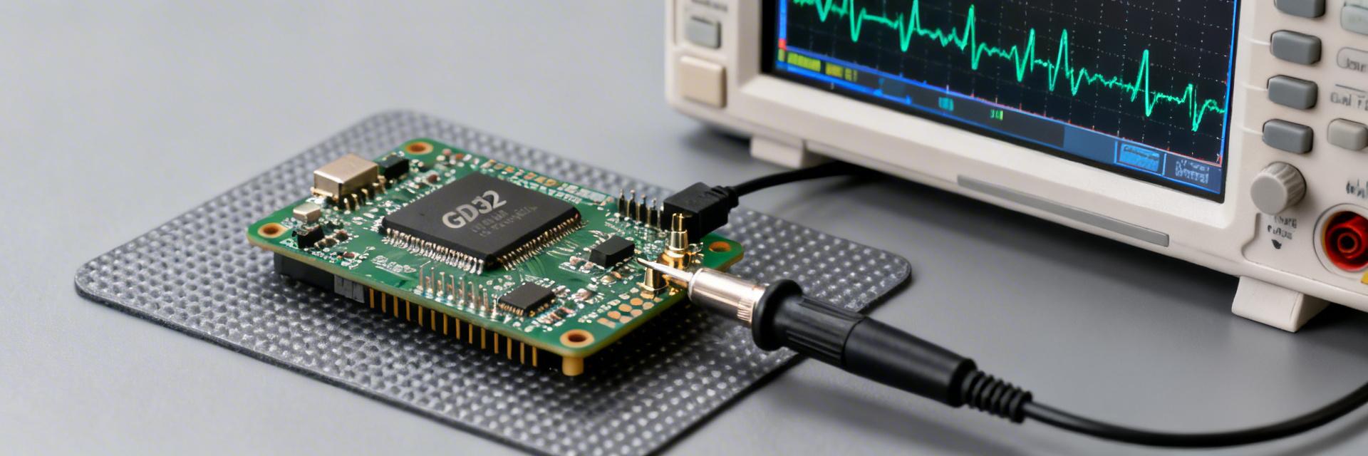
- ✔ Hardware Setup: Stable low-noise power supply, deterministic clock source, and oscilloscope verification.
- ✔ Software Stack: Consistent compiler flags (O3 optimization), documented Flash wait states, and DMA-enabled drivers.
- ✔ Metrics: Execution time (ms), throughput (MB/s), latency (µs), and thermal delta across workload cycles.
Key Summary
- The GD32F103RBT6 delivers solid Cortex-M3 compute; account for Flash wait states in integer-heavy tasks.
- Peripherals like USB FS and CAN reach spec numbers only with DMA, careful pin routing, and ISR optimization.
- Thermal and power are the main production limits; implement clock scaling and duty cycling to maintain long-term reliability.
Common Questions — Designer's Guide
How do I validate GD32F103RBT6 CPU performance for my application? +
What benchmark setup shows realistic peripheral throughput? +
Which tests detect operational limits early? +
