This article condenses the full datasheet into clear sections: quick specs, electrical characteristics and limits, a hands-on pinout guide, peripheral and memory-map highlights, and a practical hardware checklist. Readers will get precise guidance for regulator selection, decoupling, AF pin choices, and verification points without hunting through large reference tables.


GD32F105VCT6 Datasheet Breakdown: Complete Specs & Pinout
2026-02-06
Designers building connectivity-focused boards need a compact, data-driven distillation of the official device documentation. This guide extracts actionable specifications to shorten design cycles and reduce first-pass PCB re-spins.
Background & Quick Specs — GD32F105VCT6 Datasheet Snapshot
Core Architecture & Performance
The MCU is an Arm Cortex-M3-class core targeting mid-range connectivity tasks. Understanding the GD32F105VCT6 clock speed and core features lets engineers budget peripheral timings, Flash wait states, and real-time scheduling margins early in the design.
Memory & Package Variants
Choosing the VCT6 part affects available AF pins and memory map layout; designers should pick the variant that matches flash requirement and pin availability to avoid later rework.
Resource Allocation Visualization
CPU Clock (Max Efficiency)
108 MHz
Typical Power Consumption
Low Power Optimized
Electrical Characteristics & Limits
Operating Voltages
The datasheet's electrical characteristics tables give Vdd min/max and recommended operating ranges. Use these values to select a regulator with headroom for startup and inrush; place decoupling close to Vdd/Vss pins.
Absolute Maximum Ratings
Absolute limits and thermal constraints are non-negotiable. Exceeding input clamp voltages or junction temperatures risks permanent damage. Apply component derating and thermal vias under the exposed pad.
Pinout & Package Details — VCT6 Guide
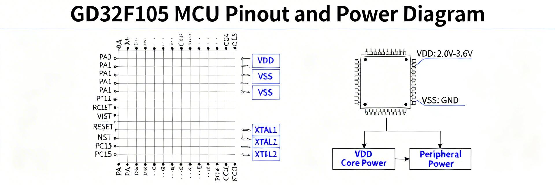
Package Diagram and Pin-Function Summary
Designers should produce a labeled pinout diagram that highlights Vss/Vdd clusters and Vref. Route Vcap and VDDA separately with local decoupling, and follow the package land pattern closely for reliable soldering. The VCT6 package (LQFP100) provides a balanced density for complex I/O requirements.
Alternate Functions & Multiplexing
For a connectivity board, reserve pins for UART console, SPI flash, and USB D+/D− early. If multiple peripherals share pins, consult the AF matrix in the datasheet to choose alternate mappings that minimize trace crossings and ease routing.
Peripheral & Memory Map Breakdown
Peripherals determine PCB and schematic needs beyond basic MCU pins. USB requires controlled-impedance differential routing and VBUS sensing; CAN needs a transceiver and fail-safe termination. Use DMA for high-throughput links and consult peripheral notes for clock source requirements.
                // Minimal Initialization Sequence

                system_clock_config();   // set PLL and flash wait states

                enable_peripheral_clock(USART1 | SPI1 | DMA1);

                configure_gpio_af(UART_TX_RX, SPI_PINS);

                init_usb_if_required();
Plan Flash wait states to match clock settings, map DMA channels to high-bandwidth peripherals, and check ADC Vref/VDDA routing to meet accuracy requirements outlined in the datasheet.
Practical Design Checklist & Troubleshooting
- ✔PCB Footprint: Place 0.1µF decouplers adjacent to each Vdd pin.
- ✔Thermal Management: Route the exposed pad to multiple ground vias.
- ✔Reset Path: Integrate a clean reset path with a capacitor or supervisor.
- ✔Verification: Expose SWD pins and power rails as test points.
- ✔Boot Mode: Use recommended resistor values for boot-mode pin states.
- ✔Debugging: Check clock gating and AF remap conflicts if peripherals fail.
Frequently Asked Questions

Contact Us
Room 1304, Building 2, Phase I, Zhuoyue city, Shangmeilin, Futian District, Shenzhen City, Guangdong Province, China.
Email
Telephone
86-0755-8320-8944