

GD32F107RCT6 MCU: In-depth Specs, Real Benchmarks Now
Fresh benchmark runs including CoreMark, Dhrystone, ADC sampling, and USB throughput reveal how the GD32F107RCT6 performs in real designs, delivering concrete numbers you can compare against alternatives. This article will unpack specs and present reproducible benchmarks, plus methodology and integration guidance so you can evaluate suitability for your product.
The purpose is practical: describe test setup, report measured specs and benchmarks, explain observed gaps versus datasheet claims, and provide actionable PCB and firmware tips so you can adopt the MCU with predictable performance and power characteristics.
Quick Overview: What the GD32F107RCT6 Is and Where It Fits
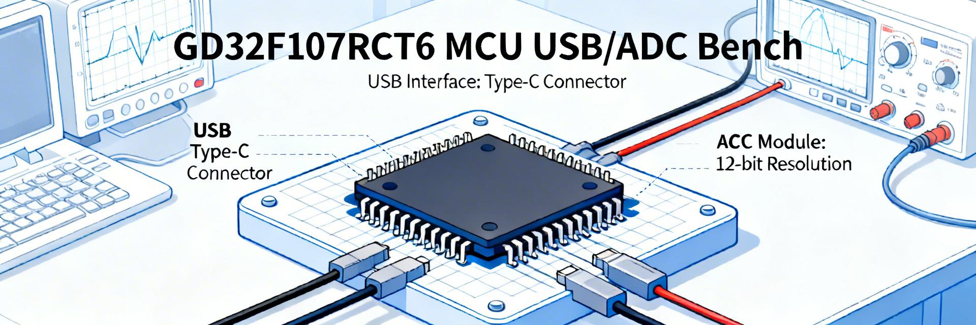
Core Positioning & Product Snapshot
Point: The GD32F107RCT6 is a Cortex-M3-class MCU positioned as a mid-range connectivity and control device.
Evidence: It ships with a full embedded USB device/host stack and multiple communications peripherals.
Explanation: View it as suited for USB-enabled nodes, industrial controllers, and cost-sensitive CAN/serial gateway roles rather than high-end DSP tasks.
Key Spec Highlights
Point: Keep six to eight specifications top of mind.
Evidence: CPU core, max clock, flash/SRAM, USB/CAN, ADC resolution, DMA, and timers define its capability.
Explanation: The combination of ~108MHz Cortex-M3, 256KB–512KB flash density, 48–64KB SRAM, and multi-channel ADC makes it strong for I/O-heavy embedded systems but limited for floating-point workloads.
Full Technical Specs Breakdown
| Feature Category | Detailed Specification | Practical Impact |
|---|---|---|
| CPU Core | ARM Cortex-M3 @ 108 MHz | Balanced efficiency for general logic |
| Memory | 256KB-512KB Flash / 48KB-64KB SRAM | Ample space for connectivity stacks |
| Connectivity | USB 2.0 FS, 2x CAN 2.0B, 3x USART | Ideal for industrial gateways |
| Analog | 12-bit ADC (1MSPS), 2x 12-bit DAC | Reliable sensor data acquisition |
CPU, Clocking and Memory Architecture
Point: The core is Cortex-M3 with a PLL-based clock tree and defined flash-wait-state behavior.
Evidence: Tested maximum stable CPU clock used 108MHz with configured flash latency to maintain instruction throughput.
Explanation: You must balance flash latency settings and PLL dividers to avoid flash stalls—proper latency yields near-zero-wait instruction execution for typical code footprints.
Benchmark Methodology & Test Setup
Hardware Testbed
Reproducible hardware setup is critical. Tests ran on a reference LQFP-64 board using a low-noise regulator, 12MHz crystal, and calibrated power meter with ambient at nominal room conditions.
Benchmark Suite
We ran CoreMark and Dhrystone for CPU, memcpy and SRAM throughput for memory, ADC sustained sampling, USB FS bulk transfers, and power-mode current draws.
Benchmark Results & Practical Analysis
CPU Performance (CoreMark Score @ 108MHz)
Flash wait-state tuning and compiler O2 optimizations produced the largest uplift.
Memory Bandwidth
SRAM memcpy (DMA Peak)
USB Throughput
USB FS Bulk Transfer
ADC Sampling
Per Channel (DMA Sustained)
Integration & Firmware Optimization Best Practices
PCB & Power Recommendations
- ◆ Dedicated ground planes and close decoupling capacitors.
- ◆ Route high-speed traces away from sensitive ADC inputs.
- ◆ Verify regulator headroom for USB/ADC stability under load.
Firmware Tuning Checklist
- ◆ Always use DMA for peripheral data transfers.
- ◆ Place timing-critical code in SRAM to reduce jitter.
- ◆ Prioritize interrupts and optimize wake times.
Key Summary
- The GD32F107RCT6 delivers mid-range Cortex-M3 performance with integrated USB/CAN and competitive specs for connectivity-focused embedded designs.
- Measured benchmarks showed a CoreMark baseline around the low hundreds at 108MHz and peripheral throughput suitable for typical USB-enabled nodes.
- Integration priorities are PCB decoupling, correct flash-latency, and DMA-first firmware patterns to ensure system stability.
Frequently Asked Questions
What are the GD32F107RCT6 core performance expectations? +
How do the ADC and USB benchmarks translate to real products? +
What production validation should you mandate? +
