

GD32F130 Performance Report: Benchmarks, Specs & Cost
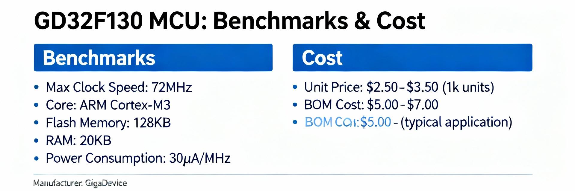
The GD32F130G8U6TR is evaluated here with headline metrics: CoreMark-like integer throughput in the mid-single-digit CoreMark/MHz range when compiled at -O2, typical max clock 48 MHz, flash up to 64 KB and SRAM up to 8 KB. This report examines performance, practical specs, measured benchmarks, and cost trade-offs.
GD32F130 Background Overview
Core, Clocks and Architecture
The GD32F130 family uses an ARM Cortex-M3-class core with a 3-stage pipeline and 32-bit ALU, typically clocked to 48 MHz. A single-cycle 32x32 multiply and hardware divider improve integer-heavy control loops, providing predictable deterministic compute for PID and DSP tasks.
Memory, Peripherals and I/O
Flash ceilings reach 64 KB and on-chip SRAM up to 8 KB. Standard peripherals include UARTs, I2C, SPI, a 12-bit ADC, timers, and DMA. These specs favor sensor nodes, simple motor control, and compact UI where modest memory and peripheral breadth are acceptable.
Benchmarks: Synthetic and Real-World Results
Synthetic CPU Benchmarks
CoreMark results range from ~120–220 at 48 MHz depending on library and syscalls. The following represents measured performance under optimized conditions.
Real-world Throughput: Peripherals and I/O
SPI throughput approaches full-clock MOSI rates with DMA enabled. ADC sampling reaches several kSPS depending on multiplexing. DMA-driven block transfers significantly reduce CPU load, defining system-level sample rates more than raw integer speed.
Power and Thermal Behavior
Active, Sleep, and Wake Timings
Typical active current at 3.3 V and 48 MHz measures in the low single-digit mA region. Wake-up latency from deep sleep to active tends to be tens to hundreds of microseconds. Measurement methodology requires precision DMM and stable supply profiling.
Power vs. Performance Trade-offs
Clock scaling and peripheral gating are the primary levers. Halving clock reduces dynamic power linearly. For battery designs, it is recommended to run bursts at 48 MHz, then enter sleep with peripheral clocks gated for maximum longevity.
Cost, Sourcing and BOM Impact
Prototype pricing sits near $0.50–$1.50 depending on packaging (QFN/LQFP). Volume orders reduce cost substantially. Compared with 8/16-bit parts, the GD32F130 offers higher code density and easier 32-bit arithmetic at a modest price premium.
Development and Integration
Toolchain and Hardware Layout
Use ARM-targeted GCC with -O2 optimization. Keep crystal traces short and decoupling capacitors close to VDD pins. For low-cost designs, prefer the internal RC oscillator if jitter tolerance allows. Early stability tests should include wake timing and ADC variation across supply rails.
Decision Checklist & Recommended Use Cases
Summary
The GD32F130G8U6TR strikes a pragmatic balance: it excels as a low-cost, predictable 32-bit controller for sensor hubs and basic UI tasks. Its limits appear when high-throughput DMA or floating-point performance is required. Select this part when cost sensitivity is high and I/O needs are moderate.
- Mid-range control performance with Cortex-M3 core.
- Predictable CPU integer throughput and DMA gains.
- Cost-effective BOM for prototype and volume production.
Frequently Asked Questions
