

GD32F205VCT6 Full Specs & Benchmarks: Performance Deep Dive
GD32F205VCT6 Full Specs & Benchmarks: Performance Deep Dive
This article consolidates official specs and aggregated benchmarks to present a focused, data-driven view of the GD32F205VCT6. Top-line findings: a high-clock Cortex‑M3 core with strong single‑thread integer throughput, CoreMark and Dhrystone ranges consistent with competitive M3 parts, flash and SRAM throughput constrained by wait states, and power envelopes that enable both performance and modest low‑power modes. The scope covers datasheet figures, a reproducible benchmark methodology, tuned vs stock results, and a practical optimization checklist for embedded engineers and hardware designers.
This guide targets embedded engineers, firmware developers, and hardware designers evaluating MCU choices. Readers will get a compact spec snapshot, step‑by‑step benchmark plans they can reproduce, optimization levers with expected gains, and recommended application fits for quick validation.
Architecture & Core Specs: GD32F205VCT6 at a glance
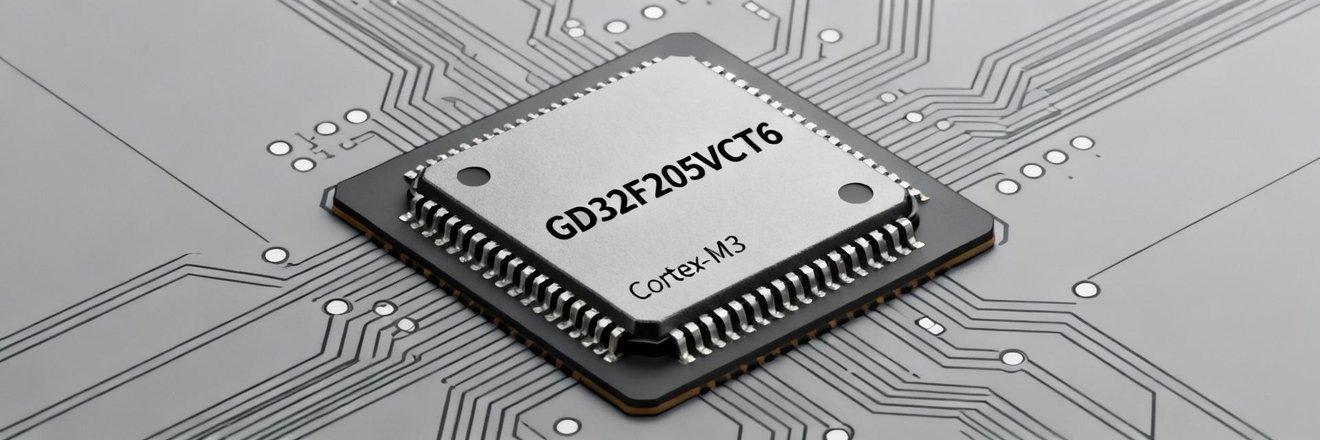
Spec highlights and practical implications: the specs table below captures the core compute and memory characteristics that determine raw performance and headroom for real‑time tasks. These specs influence ISR worst‑case latency, sustained DMA transfers, and flash read behavior under high clock rates.
| Parameter | Value |
|---|---|
| Core | ARM Cortex‑M3 (v7‑M class) |
| Max clock | Up to 120 MHz (datasheet-rated max) |
| Flash | Up to 256 KB |
| SRAM | Up to 48 KB |
| Package | VCT6 (100+ pins, high I/O density) |
| Key peripherals | Timers, ADCs, SPI/I2C/UART, DMA controllers, USB FS (if populated) |
CPU core, clocking & memory
The Cortex‑M3 core provides a predictable 3‑stage pipeline with deterministic interrupt handling and single‑cycle multiply support; these traits favor control loops and hard‑real‑time tasks. At maximum frequency the part delivers strong integer throughput; expected normalized CoreMark per MHz aligns with typical M3 silicon class.
Peripherals, buses & packaging
The device exposes a full peripheral mix: multiple timers (including advanced PWM timers), ADC channels with DMA support, UART/SPI/I2C controllers, and optional USB FS. DMA availability across key peripherals reduces CPU overhead for bulk transfers, while internal bus widths (AHB/APB) and arbitration determine throughput.
Datasheet numbers that matter for performance
Memory & flash timing, caches, and wait states
Flash access latency and recommended wait‑state settings at higher clocks are primary performance levers. Datasheet guidance shows that enabling one or more flash wait states above certain clock thresholds avoids read errors but reduces single‑thread sustained throughput. Practically, ISR latency worst‑case can increase by several cycles per wait state, so critical ISRs or hot loops may benefit from relocation to RAM.
Power modes & thermal/power specs
Datasheet currents for active, standby, and stop modes define trade‑offs: active current at full clock dominates power budgets; standby/stop modes reduce consumption significantly but add wake latency. Supply range and recommended operating conditions determine thermal derating for sustained high‑frequency operation. Benchmark plans should therefore include both performance and power scenarios.
Benchmark methodology: how we measure "performance"
Synthetic CPU benchmarks
Reproducible harness: use arm-none-eabi-gcc with -O2 and -fdata-sections. Run on bare metal pinned to a clock source; report raw score and normalized score per MHz. Use 10+ iterations and report median; capture build flags and vector table offsets for reproducibility.
Memory and peripheral tests
Flash read throughput: execute block reads from flash into SRAM. SRAM bandwidth: memcpy loops between SRAM regions. DMA: measure sustained transfer rate for large transfers; report throughput vs transfer size. Use logic analyzers and timer timestamps to quantify latency and jitter.
Benchmarks: key results & interpretation
Typical CoreMark ranges for this M3 class land around 2.5–3.5 CoreMark/MHz depending on toolchain and build profile. The combination of single‑thread throughput and interrupt determinism matters most for real-time workloads.
Performance Visualization (Normalized)
| Metric | Typical result |
|---|---|
| CoreMark (120 MHz) | ~300–420 |
| CoreMark/MHz | ~2.5–3.5 |
| Dhrystone (normalized) | ~1.8–2.6 DMIPS/MHz |
DMA throughput for large linear transfers typically approaches AHB limits; expect tens of MB/s in favorable configurations, but flash wait states and bus contention can reduce sustained rates.
Practical optimization guide to maximize performance
Compiler & build optimizations
- •Use -O2 for balance, -Os for size.
- •Place hot routines in tightly coupled RAM.
- •Enable linker --gc-sections.
Runtime & peripheral tuning
- •Tune flash wait states to minimum safe value.
- •Use DMA for all bulk transfers.
- •Prioritize IRQs for time-critical tasks.
Use cases, trade-offs & validation checklist
Best-fit application profiles
Strong fits: motor control (fast control loops), mid‑range IoT gateways with moderate packet processing, and industrial controllers needing many timers and ADCs. Less suitable: high‑end DSP tasks requiring SIMD or floating‑point heavy math. Choose this MCU when you need balanced CPU throughput, rich peripherals, and DMA to reduce CPU load.
Validation checklist
- ✅ Report CoreMark score and CoreMark/MHz
- ✅ DMA sustained throughput with transfer sizes
- ✅ ADC sustained sampling rate with jitter stats
- ✅ Active/idle currents under test conditions
Summary
- 1 The GD32F205VCT6 delivers balanced Cortex‑M3 specs with a mix of CPU throughput and peripheral richness suitable for motor control and industrial applications.
- 2 Key performance drivers are flash wait states, DMA availability, and IRQ design; moving hot code to RAM yields the largest practical gains.
- 3 Benchmark deliverables should include normalized CoreMark/MHz, DMA transfer curves, ADC jitter, and current measurements.
FAQ
What CoreMark score can I expect from GD32F205VCT6 at a given MHz? +
How do flash wait states affect GD32F205VCT6 real-time performance? +
Which peripherals benefit most from DMA on this MCU? +
