

GD32F205VGT6 Technical Report: Real Benchmarks & Insights
Real Benchmarks & Engineering Insights for Embedded Systems
This report presents a hands-on, data-driven benchmark suite for the GD32F205VGT6 MCU, covering CPU throughput, memory/flash behavior, peripheral latency (ADC, UART, SPI, I2C), DMA and interrupt interactions, and power at representative operating points. The test matrix uses multiple runs on the same testboard with controlled clock and supply conditions to emphasize reproducibility. Our benchmark suite highlights where the device outperforms expectations in sustained I/O and where it shows limits in flash write throughput, offering practical value to embedded engineers and procurement teams.
Device Overview & Key Specifications
Core & Memory Profile
The MCU centers on a high-performance 32-bit core designed for deterministic embedded workloads. Operating at up to 120 MHz with an ARM Cortex-M3 class pipeline, it is paired with 512 KB Flash and 96 KB SRAM. These resources define the ceiling for integer throughput and interrupt responsiveness.
Peripheral & IO Summary
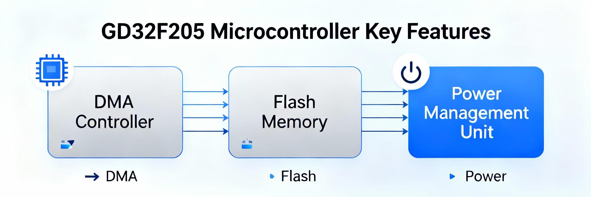
Features multiple high-speed masters: SPI engines, UARTs, I2C controllers, and ADC with sample sequencers. A flexible internal clock tree routes PLL or HCLK sources, while multi-channel DMA ensures throughput is maintained during heavy stress tests.
Benchmark Methodology & Test Matrix
Testbed Setup
Tests were executed on a single populated testboard with isolated power rails and decoupling at regulator outputs. Clock was fixed to 120 MHz using O2 optimization flags to ensure reproducibility across third-party labs.
Performance Metrics (Visualized)
Raw Benchmark Results
Real-World Use Cases & Scenarios
Implementation Tips & Tuning
- ✔ Optimize Flash: Place high-frequency ISR code in SRAM to eliminate flash-wait states during critical timing.
- ✔ DMA Chaining: Use DMA for sustained SPI/UART transfers to keep CPU utilization low for background tasks.
- ✔ Thermal Stability: Always allow the MCU temperature to stabilize before taking final power measurements.
Key Summary
- Solid integer throughput and effective DMA-driven I/O for sustained multi-megabit transfers.
- Flash access patterns dominate worst-case stalls; buffer critical routines to SRAM.
- Active I/O and full-speed compute draw low-hundreds of milliwatts—validate workload specific power before commit.
Frequently Asked Questions
What workload types reveal the most about MCU suitability?
How should engineers validate power numbers for a design using this MCU?
Which tests confirm DMA is configured correctly?
