

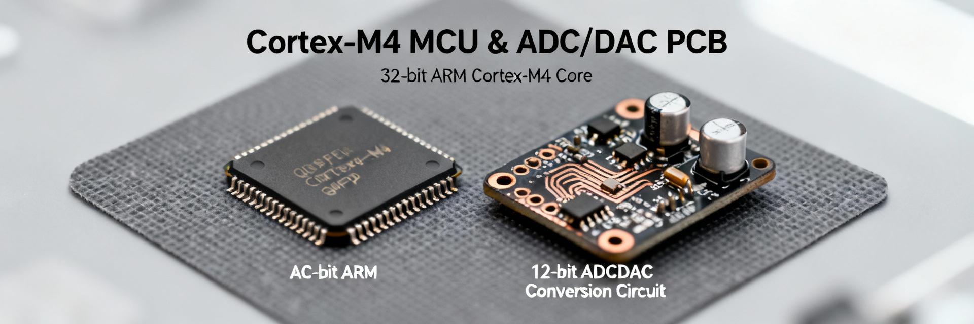
The GD32F303CGT6 features a high-performance Cortex-M4 core running up to 120 MHz, equipped with up to 256 KB flash, a 12-bit ADC, and dual 12-bit DACs. Operating within a 2.6–3.6 V supply range, this MCU is precision-engineered for motor control, industrial sensing, and advanced peripherals.
Background & Device Overview
Family Positioning & Part-Code Decode
Point: The device sits in the mainstream Cortex-M4 family optimized for mixed-signal embedded control. Evidence: Datasheet part numbering and family tables list memory, package, and suffix variants. Explanation: Designers should use the part-code table to confirm flash/SRAM, package pinout, and temperature grade before schematic capture.
Typical Applications & Design Intent
Point: Target uses include real-time motor control, sensor acquisition nodes, and audio/analog processing. Evidence: Integrated ADC/DAC, multiple timer types, and DMA are highlighted in peripheral summaries. Explanation: Matching application needs to on-chip features shortens bring-up time significantly.
Core Specs Snapshot
CPU & Memory Architecture
The core is a Cortex-M4 with FPU and DSP instructions. Flash is available up to 256 KB.
Design Note: Designers must set flash latency according to the clock frequency and consult the clock tree for PLL VCO ranges to ensure system stability.
Digital I/O & DMA
GPIOs support multiple Alternative Functions (AF) and high-speed drive.
Efficiency Tip: For high-throughput UART/SPI, route data via DMA and reserve high NVIC priority for time-critical ISRs to minimize jitter.
Analog & Mixed-Signal Peripherals
Signal Chain Note: Use hardware triggers for deterministic sampling. Interconnect diagrams in the datasheet specify how timer events can trigger ADC conversion without CPU intervention.
Case Study: Motor Control
- ✦ Peripheral Mapping: Map ADC+DMA for phase sensing and advanced timers for PWM.
- ✦ Synchronization: Reserve a timer channel per PWM phase to maintain synchronized control loops.
- ✦ Validation: Capture ISR-to-ISR jitter and verify ADC acquisition vs datasheet sample time.
Power, Packaging & Environmental Specs
Supply Rails & Consumption
Operates across 2.6–3.6 V. Includes multiple low-power modes.
Guidance: Estimate battery life by duty-cycling active sampling and using deep sleep between wakeups. Validate measured currents against datasheet table values.
Thermal & PCB Layout
Follow ADC input routing and local decoupling near VDD pins. Keep crystal traces short to minimize noise.
Guidance: Consult thermal derating curves to ensure the board maintains margins under heavy computational load.
Summary
- The GD32F303CGT6 combines a Cortex-M4 CPU, 12-bit ADC, and dual 12-bit DACs with ample timers and DMA.
- Record max core frequency, flash/SRAM sizes, and ADC acquisition time for accurate performance budgeting.
- Use the datasheet part table early to lock pinout and thermal constraints during the hardware design phase.
