

GD32F303RCT6 Specs Snapshot: Performance & Peripherals
The GD32F303RCT6 delivers a 32-bit Cortex-M4 core with FPU running up to 120 MHz, positioned as a balanced high-speed MCU for real-time control and mixed-signal applications.
Quick Specs Snapshot & Architecture Overview
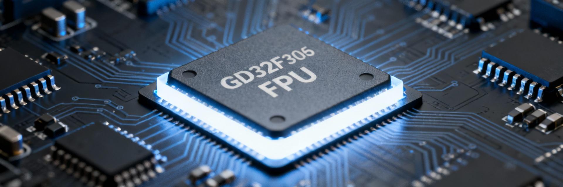
Core & Clocking Essentials
The device utilizes an ARM Cortex-M4 core with a single-precision FPU and DSP extensions, reaching speeds up to 120 MHz. Clocking relies on internal RC and external crystal sources with flexible PLL options and a hierarchical clock tree structure.
Memory & Electrical Envelope
With 256 KB Flash and 48 KB SRAM, this MCU fits sophisticated firmware layouts. The VDD range of 2.6–3.6 V and LQFP-64 packaging provide a robust deployment envelope for commercial and industrial applications.
| Hardware Item | Technical Value |
|---|---|
| Core Architecture | ARM® Cortex®-M4 with FPU & DSP |
| Maximum Clock Speed | 120 MHz |
| Flash Memory | 256 KB |
| SRAM Capacity | 48 KB |
| Package Type | LQFP-64 (10x10 mm) |
| Operating Voltage (VDD) | 2.6 V – 3.6 V |
Performance Profile & Benchmarking Guidance
Quantifying throughput and power is essential for system budgeting. The Cortex-M4 core provides strong floating-point and DSP throughput, visible in standard CoreMark scores.
CPU Performance & Synthetic Benchmarks (Typical Values)
Power, Thermal Behavior & Real-World Throughput
Active versus low-power currents change dramatically based on peripheral load. It is critical to measure current with a high-precision meter during representative modes, such as periodic ADC sampling or PWM motor driving, while monitoring the PCB thermal gradient.
Peripherals Breakdown: Timers, Analog, and Comms
The GD32F303RCT6 peripheral set is designed for mixed-signal control systems, offering a rich matrix of capabilities.
| Peripheral Type | Key Capability | Typical Use Case |
|---|---|---|
| Advanced Timers | PWM channels, dead-time insertion | Motor control, power stages |
| Analog (ADC) | Multiple channels, high-speed sampling | Sensor fusion, control loops |
| DAC / Comparators | Analog outputs / threshold monitoring | Signal generation, protection |
| Serial Comms | USART / SPI / I2C / USB (DMA support) | Telemetry, sensors, UI interfaces |
Development & Integration Checklist
                enable_HSE();

                configure_PLL(mult=10);

                set_system_clock(120MHz);

                enable_peripheral_clock(TIM1 | ADC1 | DMA1);
Hardware Integration Tips
- ✔ Do: Place 0.1 µF decouplers within 1–2 mm of VDD pins.
- ✘ Don't: Route noisy switching traces under the ADC analog area.
- ✔ Do: Provide a solid AGND plane for ADC return paths.
Firmware Strategy
Pick a toolchain with hardware FPU and CMSIS support. Plan linker sections for RAM/Flash management and only enable peripheral clocks when necessary to optimize power consumption.
Quick Selection FAQ for Engineers
1. Is the CPU performance sufficient for my algorithms?
2. How much memory is available for firmware and OTA?
3. Does it support advanced motor control features?
4. What are the communication interface options?
