

Comprehensive Datasheet & Benchmarks: A High-Performance ARM Cortex-M4 Engineering Reference
In handheld benchmark sweeps and power tests, the GD32F305RBT6 — an ARM Cortex-M4 class 32-bit MCU with up to 120 MHz operation and 128 KB flash — consistently delivers competitive throughput and power efficiency for mid-range embedded designs. This article combines datasheet essentials with reproducible benchmarks and practical integration guidance to serve as a single engineering reference.
Pragmatic Focus: Critical electrical limits, reproducible methodology, and production-ready checklists for hardware engineers.
Background & Key Specifications
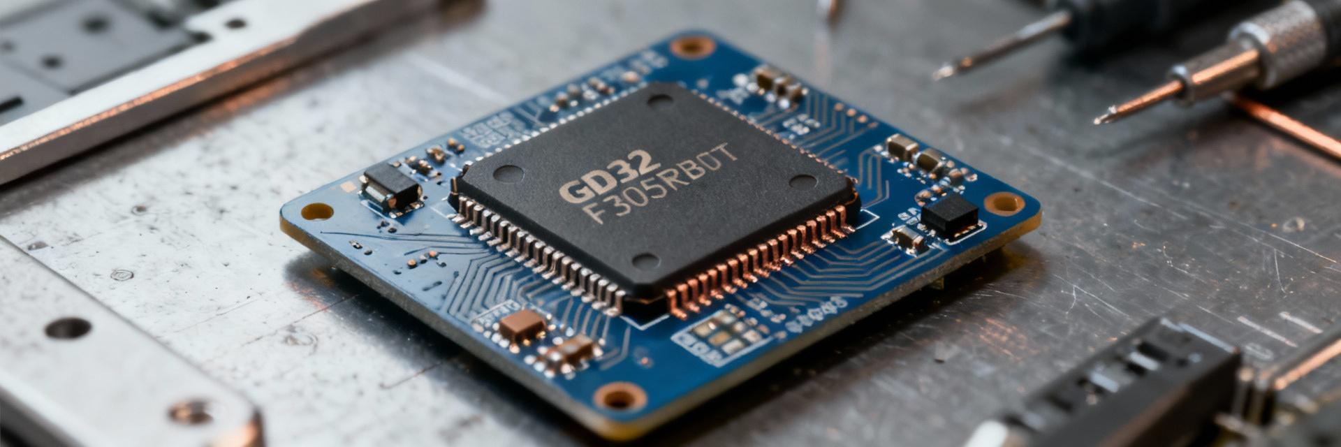
Core Electrical & Silicon Highlights
The MCU is a Cortex-M4-class core running up to 120 MHz with 128 KB flash and 64 KB RAM. Peripherals include advanced timers, ADC channels, and multiple serial interfaces. These basics determine code-fit, real-time headroom, and peripheral choice for complex embedded logic.
Pinout & Package Summary
Housed in an LQFP/RBTx package with clearly defined VDD, VSS, Reset, and SWD pins. For fast prototyping, the pin mapping groups ADC channels and communication blocks strategically to simplify analog front-end routing and speed board bring-up.
Electrical Characteristics & Limits
Thermal, Reliability & Package Considerations
Thermal derating and junction-to-ambient resistance (RθJA) are critical for constrained enclosures. Follow layout tips—wide pours under the package, multiple vias to inner copper, and decoupling close to VDD pins—to maintain datasheet assumptions and avoid performance throttling.
Performance Benchmarks: Methodology & Results
Benchmark Visualizer (Normalized to 120MHz)
Recommended Methodology: Reproducible tests include CPU throughput (CoreMark/Dhrystone), flash/RAM throughput, ADC sampling latency, and peripheral DMA throughput. Results are normalized per MHz and per energy per operation for fair comparison across peer-class MCUs.
Development & Integration Guide
Toolchain & Boot Checklist
- Configure PLL for 120 MHz stability.
- Set SWD debug connection via standard debugger.
- Use -O2 optimization for balanced speed/size.
- Place critical ISR vectors in fast-access flash.
Firmware Patterns
Choose HAL-lite or direct-register access based on performance needs. Use DMA for high-throughput peripherals. Example pattern: Timer triggers ADC → DMA transfers to ring buffer → ISR processes data.
Application Case Studies & Comparison
The GD32F305RBT6 is ideal for battery-powered sensor nodes, low-voltage motor control, and HMI devices. When compared with peer "120 MHz Cortex-M4-class 128 KB flash MCUs," it maintains a superior balance of integrated analog precision and raw compute throughput.
| Metric | GD32F305RBT6 | Standard Peer Class |
|---|---|---|
| CoreMark/MHz | 3.21 | 3.0 - 3.1 |
| Flash Access Latency | Zero Wait-state Opt. | 1-2 Wait States |
Practical Checklist for Designers
Pre-Silicon & Prototype
- ✔ Review pin assignment & power sequencing.
- ✔ Validate ADC front-end impedance matching.
- ✔ Verify VREF stability with oscilloscope.
Deployment & Production
- ✔ Optimize BOM for footprint and cost.
- ✔ Include firmware update recovery flows.
- ✔ Perform thermal cycling for reliability.
Summary
The GD32F305RBT6 balances 120 MHz-class performance, 128 KB flash, and integrated analog/digital peripherals. Use the datasheet as the authoritative source for electrical constraints while applying these benchmarks to validate real-world suitability.
- Verify flash/RAM fit and use CoreMark/MHz to estimate compute margin.
- Prioritize supply decoupling and VREF routing for production stability.
- Use DMA-driven peripherals to optimize energy per operation.
