

GD32F305VCT6: Pinout & Key Specs — Quick Data Brief
A compact, engineer-focused snapshot for quick board-level verification, mapping the Cortex-M4 core capabilities to practical hardware implementation.
The GD32F305VCT6 pairs a Cortex-M4-class core with up to 120 MHz operation, featuring 256 KB of flash and 96 KB of SRAM. This brief facilitates rapid schematic validation, highlighting critical pin functions and power limits necessary for a smooth first power-up.
Quick Technical Snapshot
Core & Memory Performance
Supports RTOS kernels and moderate DSP routines. Ideal for networking stacks and UI telemetry.
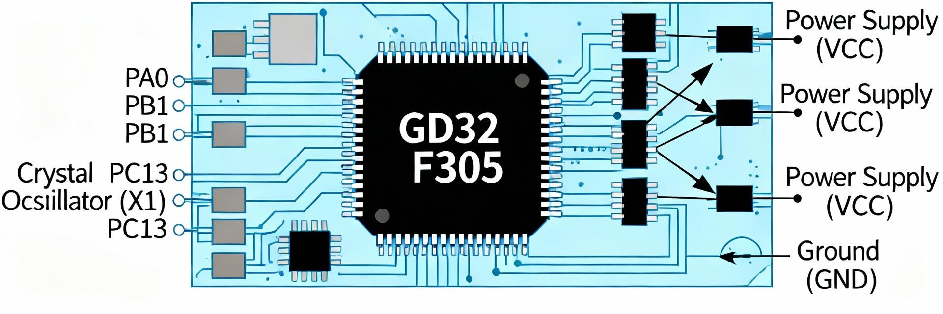
Package & Power Rails
Designed in a 100-pin LQFP package, the VDD range is 2.6–3.6 V. Engineers should implement robust decoupling close to each VDD/VSS pair and isolate analog ground paths to maintain ADC/DAC precision.
Pinout Overview: Package & Groups
Grouped Functions
- ◈ Power: VDD, VSS
- ◈ Analog: ADC, DAC Channels
- ◈ Comms: USB D+/D-, CAN, UART
- ◈ Control: NRST, BOOT0, EXMC
Critical Verification
Annotate alternate-function conflicts on schematics. Ensure BOOT0 is correctly pulled to avoid unintended boot modes during flashing or debugging cycles.
Electrical & Peripheral Specs Deep-Dive
| Parameter | Typical Range / Note |
|---|---|
| VDD Operating | 2.6 – 3.6 V |
| Max CPU Frequency | 120 MHz |
| Standby Current | Datasheet-specified μA-range (board-level measure) |
| Temperature Range | Industrial or Extended (Verify per variant) |
| Mixed-Signal | 12-bit ADC, Dual 12-bit DACs, Advanced PWM Timers |
Connectivity & Memory
USB D+/D- requires differential routing and VBUS sensing. For EXMC (External Memory Controller), ensure parallel bus signals for displays or PSRAM are documented with appropriate pull-ups and series resistors to manage signal integrity.
PCB Layout Strategy
Place decoupling capacitors immediately adjacent to power pins. Keep high-current traces away from analog ADC inputs and implement a star-ground configuration to minimize noise injection during high-speed switching.
Quick-Start & Design Checklist
