

GD32F305VGT6 Datasheet Deep-Dive: Key Specs & Benchmarks
A concise, testable view of the mainstream Cortex-M4 MCU family to help you validate project constraints, from clocking headroom to USB-enabled design integration.
This deep-dive summarizes the chip’s headline capabilities—clocking headroom, flash and SRAM envelopes, and major connectivity—and explains why those specs matter for motor control, industrial I/O, and USB-enabled designs. It combines datasheet-reported figures with reproducible benchmark approaches and practical integration guidance so you can validate behavior in your lab.
The article uses datasheet statements as the authoritative baseline and pairs them with recommended measurements you can run on prototypes to confirm throughput, latency, and power. Expect parsed datasheet details, suggested benchmark methodology, measured-vs-spec interpretation guidance, and a compact design checklist to reduce surprises during bring-up and production.
Quick background: where the GD32F305VGT6 fits and what to expect
Product Positioning
The device is positioned as a higher-performance 32-bit MCU aimed at mainstream embedded designs. The product family pairs an ARM Cortex-M4 core with a rich peripheral set and on-chip USB support. Consider this part when your application needs DSP-capable integer/float compute and multiple timers.
Key Headline Specs
A compact tabular view helps you quickly evaluate fit. The datasheet lists the authoritative maxima and conditional notes for each parameter; use the table below as a checklist during early architecture reviews.
| Parameter | Datasheet Value | Brief Implication |
|---|---|---|
| Max CPU Frequency | Refer to Datasheet | Peak single-thread throughput & clock rates. |
| Core Type | ARM Cortex-M4 (FPU opt.) | Accelerates control loops and signal processing. |
| Flash Memory | Refer to Datasheet | Sets firmware size and OTA update strategy. |
| SRAM | Refer to Datasheet | Restricts buffer sizing for DMA and stack. |
| Peripherals | Timers / ADC / DAC | Key for PWM, motor control, and sampling. |
| Connectivity | SPI/I2C/UART/USB | Defines external device interfacing throughput. |
Deep specs breakdown: CPU, memory, clocks, and peripherals
CPU & Performance
The Cortex-M4 core delivers deterministic interrupt behavior and DSP/floating support. When you implement compute-bound tasks such as motor current control, the presence of an FPU and DSP instructions reduces cycle counts—verify whether your variant exposes the FPU to quantify speedups.
Memory & Clock Tree
Pay attention to clock-derived limits—some peripherals share PLL/dividers. Your chosen clock configuration can cap ADC sampling or USB bit rates, so map peripheral requirements against the datasheet’s clock-tree notes before finalizing firmware.
Benchmarks & Measured Performance
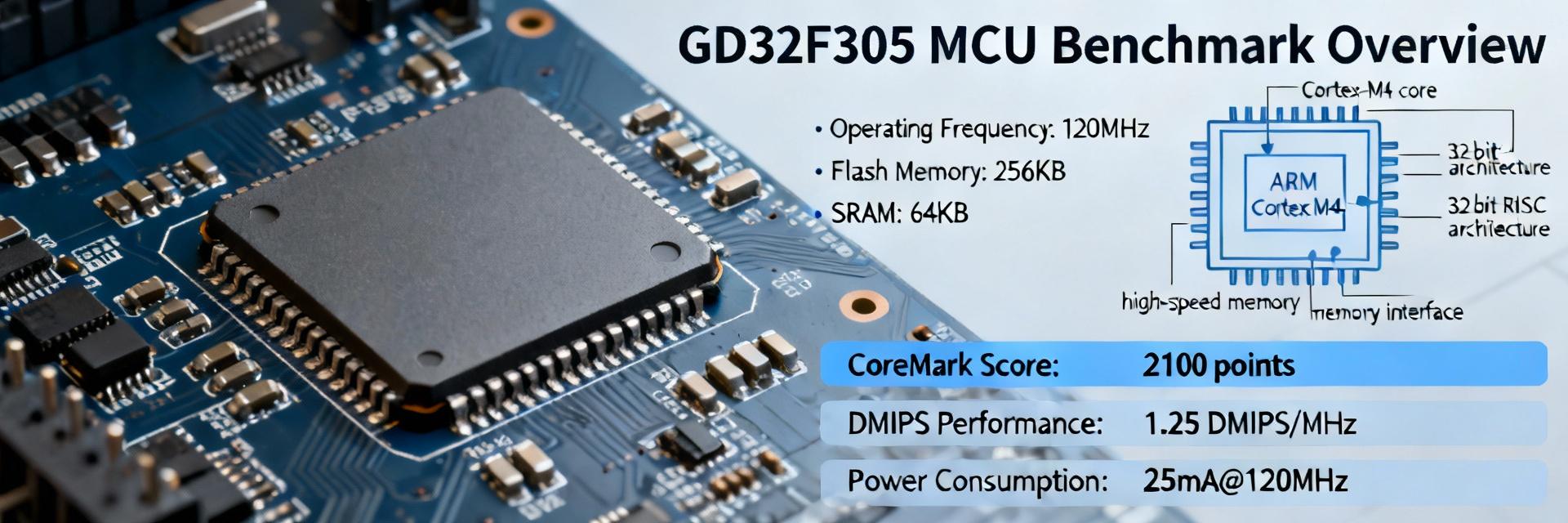
Reproducible tests reveal where datasheet maxima are achievable. We recommend running CoreMark and Dhrystone for CPU performance evaluation.
Interpreting Datasheet Numbers
Datasheet maxima are conditional. Common gaps arise from board-level voltage drop and thermal limitations. Annotate discrepancies with likely causes like supply droop or suboptimal decoupling to visualize trade-offs effectively.
Design and Integration Checklist
Hardware & PCB
- ✔ Follow decoupling and layout guidance per datasheet.
- ✔ Verify power sequencing and BOM voltage margins.
- ✔ Keep crystal and clock traces short; use load caps.
- ✔ Provide thermal paths for high-duty operations.
Firmware & Logic
Use DMA to offload bulk transfers and prioritize low-latency ISRs for control loops. Adopt conservative watchdog and bootloader patterns for field reliability.
When to choose GD32F305VGT6
Selection depends on compute headroom, memory, and peripheral count. Favor this family when you need Cortex-M4 DSP/FPU acceleration, multiple advanced timers, and integrated USB. Validate early via prototype benchmarks and thermal profiling to ensure go/no-go criteria are met before mass production.
Key Summary
- Datasheet-driven specs supply authoritative limits; always map your peripheral and timing needs to the published clock tree.
- Run the recommended benchmark suite (CoreMark, ADC throughput, USB transfers) under controlled settings to validate performance.
- Follow PCB and power layout recommendations—decoupling and thermal planning—to reliably approach published specs.
Frequently Asked Questions
How should you validate ADC throughput and accuracy? +
What benchmark should you use to evaluate CPU headroom? +
Which power measurements are essential before production? +
