

GD32F305ZET6 Technical Summary: Pinout & Specs Guide
Recent datasheet aggregations and benchmark summaries place the GD32F305ZET6 among current high-performance Cortex-M4-class microcontrollers for mid- to high-end embedded designs. This introduction frames device relevance for engineers selecting a 32-bit MCU with an emphasis on peripheral richness, I/O density, and real-world implementability in constrained cost targets.
The goal of this brief is to deliver a compact, actionable technical summary focused on pinout, electrical and peripheral specs, and practical design guidance oriented to US engineering teams planning prototypes and production.
Background & Device Positioning
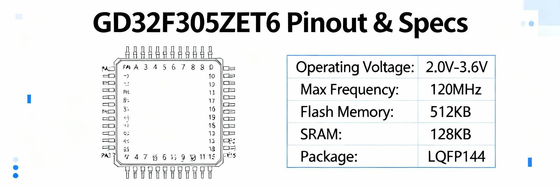
Device Overview: Target Applications
The GD32F305ZET6 is a Cortex-M4-class MCU positioned for mid/high performance embedded applications. Evidence from datasheet summaries and benchmark collections characterize it by a high core performance tier, multi-channel ADCs, abundant serial interfaces, and a large LQFP package option with substantial I/O. These traits make the device suitable for industrial controls, motor control, audio front-ends, and HMI panels where both CPU throughput and peripheral mix are critical.
Key Differentiation & Selection Rationale
Selection rationale centers on performance-per-cost, peripheral mix, and I/O density. Practical project experience shows parts with this profile reduce board-level glue and often eliminate external microcontrollers for complex I/O tasks. The engineer should weigh the MCU's integrated ADC/DAC, timer/PWM count, and multiple serial ports against system cost and power budget.
- Applications needing DSP-friendly core
- Multiple ADC channels requirement
- USB/Serial heavy connectivity
- Higher pin count increases PCB complexity
- Increased thermal and power considerations
| Attribute | Suggested Compare Field |
|---|---|
| Clock | Core frequency (indicative) |
| Flash | Max program memory |
| RAM | On-chip SRAM |
| ADC | Resolution / channels |
| Serial ports | USART/SPI/I2C counts |
Detailed Specs Breakdown
Core, Memory, Clocks & Electrical Specs
Engineers must capture core, memory, clock, and electrical envelopes early. Official datasheets list core frequency limits, flash and SRAM capacities, and VDD range. For PCB design, extract exact numeric limits and confirm them during BOM review.
| Parameter | Design Action |
|---|---|
| Core Frequency | Design to max reported core clock in datasheet |
| Flash / SRAM | Allocate memory regions and bootloader space |
| Voltage Range | Select regulator and decoupling per datasheet limits |
| Power Modes | Plan sleep/wakeup and RTC domains |
Peripherals, Timers & Comms
Peripheral count and capability commonly determine real system cost. The device integrates multiple USART/SPI/I2C interfaces, multi-channel ADC(s), timer/PWM units, DMA channels, and common USB/CAN support. The engineer should map expected peripheral usage to available instances and verify DMA channels for bulk data paths.
Pinout & Package Mapping
Pinout Overview and Diagram Guidance
Understanding the pinout is essential for reliable multiplexing and signal integrity. The LQFP package pinout shows VDD/VSS distribution, VREF pins, boot pins, and dedicated high-current I/O. Prioritize clear labeling of power pins and keep VREF isolated.
Pin Function Tables & Recommended Assignments
A disciplined pin assignment prevents mux conflicts and eases routing. Assign UART TX/RX to pins with simple routing to debug headers; reserve pins with stronger drive for PWMs.
| Pin Group | Package # | Primary | Alternate | Notes |
|---|---|---|---|---|
| PAx | Multiple | GPIO / UART1_TX | SPI1_SCK | High-speed signals |
| PBx | Multiple | ADC_INy | GPIO | Keep short, near VREF |
Practical Design Examples & PCB Layout Tips
Minimal System Schematic
- Power Rails: Regulator, bulk and decoupling caps (0.1 μF).
- Reset and Boot: Pull resistors and test points.
- Clock: Internal RC vs. External crystal (8-25MHz).
- Debug: standard SWD 2x5 or 2x3 header.
PCB Layout & EMI
- Place decoupling caps within 2–5 mm of VDD pins.
- Use an uninterrupted ground plane for signal integrity.
- Route crystal traces as a short symmetric pair.
- Controlled impedance for USB and CAN lines.
Quick-Reference Checklist & Testing
Pre-production Checklist
Debugging Tips: Use SWD to halt the core and toggle known GPIOs. Confirm reset behavior with an oscilloscope and isolate peripherals by disabling unused muxed functions to identify the fault domain.
Summary
In short, the GD32F305ZET6 delivers a Cortex-M4-class balance of performance and peripheral integration that suits industrial, motor, and HMI applications.
- Confirm core and memory requirements against reported specs before finalizing bootloader partitioning.
- Prioritize pin assignments: reserve dedicated timer and high-drive pins for motor/PWM applications.
- Follow layout rules: decouple each VDD pin closely and maintain a solid ground plane to reduce EMI.
Frequently Asked Questions
What are the key electrical specs and where should engineers confirm them? +
How should one approach pinout selection for high-speed interfaces? +
What quick tests confirm a board’s basic health after first assembly? +
