

GD32F350C8T6 Datasheet Deep Dive: Pinout & Key Specs
Key Technical Specifications
Pinout & Package Strategy
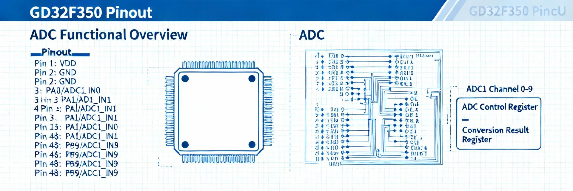
The C8T6 package is a compact option with multiplexed pins serving GPIO, ADC inputs, timers, and serial peripherals. Critical pins like VREF and VSSA must be handled with care to ensure analog precision. Study the pin map early to avoid multiplexing conflicts between UART, SPI, and high-speed ADC inputs.
Power, Clocks & Reset
Reliable operation starts with power integrity. Place 0.1 μF ceramic decouplers at every VDD pin and a 1 μF bulk capacitor on the main rail. For precision sampling, use an external crystal plus PLL to maximize ADC throughput and ensure deterministic timing across all communication blocks.
Peripherals & Implementation Guide
Analog Performance (ADC/DAC)
Maximizing accuracy requires input anti‑alias filtering and low‑noise references. Tie VREF to a stable source with local decoupling to allow the 12‑bit SAR to settle correctly according to datasheet timing limits.
Timers & Communication
Leverage DMA for high‑sample ADC workflows. Reserve dedicated PWM timer pins for motor control and consult peripheral timing tables to set baud rates for UART, SPI, and I2C interfaces accurately.
PCB Integration Checklist
Example A: Sensor Node
- Minimize active clocks to save power.
- Sequence power to sensors after VREF is stable.
- Route ADC inputs away from switching regulators.
Example B: Motor Control
- Match PWM trace lengths.
- Isolate gate‑drive signals.
- Separate analog ground plane with star‑point connection.
Rapid Troubleshooting Checklist
Verify VCC/VREF under load
Check oscillator stabilization
Confirm pin logic levels
Check debugger connectivity
Summary
The GD32F350C8T6 combines Cortex‑M4 performance with a flexible analog front end. Its pinout and package choices drive analog accuracy and peripheral availability. Key takeaways for integration include:
- Pinout Priority: Reserve VREF and AGND early; avoid multiplexing conflicts on noise-sensitive ADC channels.
- Decoupling: Place 0.1 μF ceramics at each VDD and a bulk 1 μF on the main rail.
- Clock Stability: Use an external crystal for high-precision sampling and respect startup delays.
Frequently Asked Questions
How should I place VREF and AGND to optimize ADC accuracy?
What are the first checks on initial power‑up if the MCU does not respond?
How can I reduce ADC noise in a mixed‑signal design?
