

GD32F350CBT6 Datasheet: Complete Electrical Specs & Pinout
This practical guide focuses on measurement conditions, recommended schematic patterns, and layout tips US hardware teams use during prototype validation. The article is organized to help engineers locate authoritative values, interpret electrical tables fast, and map those numbers into decoupling, power sequencing, and pin assignment decisions that reduce rework risk on first silicon.
Background: What the GD32F350CBT6 Datasheet Covers
Document Scope & Revision Notes
Point: The datasheet is the authoritative source for absolute ratings, recommended operating conditions, and electrical characteristics.
Evidence: Datasheets typically include a revision string and document date on the cover page and a revision history table.
Explanation: Always record the datasheet revision used for procurement and testing; check errata for behavioral changes and measurement notes.
How to Read Electrical Tables Quickly
Point: Electrical tables use columns such as Condition, Min/Typ/Max, Units, and Test Notes.
Evidence: Designers focus on absolute maximums and recommended operating ranges first, then typical values for power budgeting.
Explanation: Use Min/Max for margin checks and Typical for expected behavior. Pay attention to footnotes that change interpretation.
Key Electrical Specifications
Supply Voltage Range (VDD)
Power & Consumption
Identify VDD/VSS and VDDA supply ranges. Use datasheet specified test conditions (e.g., CPU halted, flash sleep) to reproduce current figures. Place decoupling close to each VDD pin.
Clocks & Performance
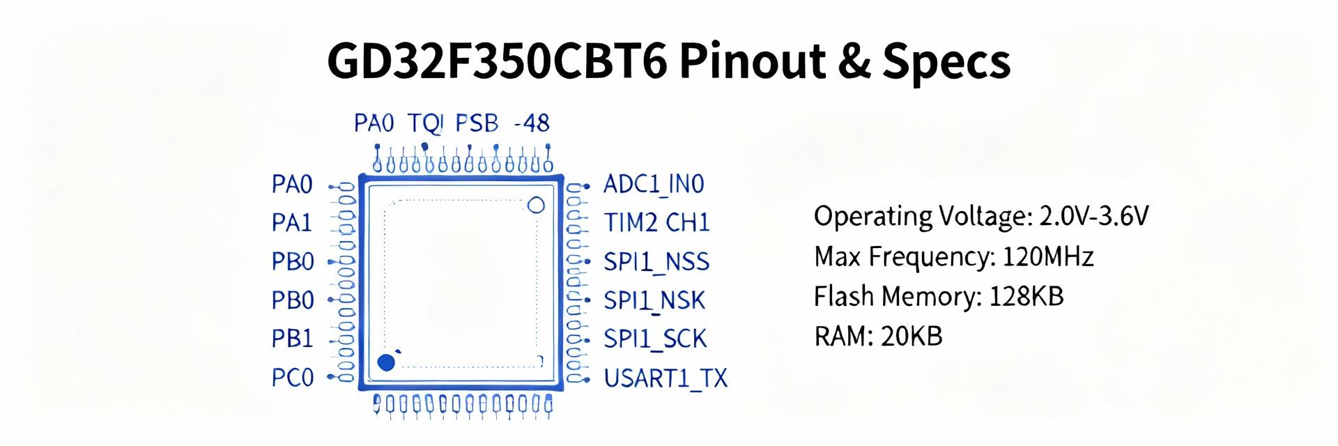
Note core max frequency (~108 MHz) and flash read-wait states. Include worst-case oscillator startup for brown-out recovery design and ISR critical timing.
Pinout & Package Details
Application Circuits & PCB Best Practices
Decoupling Strategy
- 0.1 μF caps within 1–2 mm of each VDD pin.
- 2.2–10 μF bulk capacitor near regulator output.
- RC or pi filter on VREF for ADC noise sensitivity.
Layout & Thermal
- Route analog inputs away from high-speed clocks.
- Tie thermal pad to inner planes for heat spreading.
- Keep high-speed traces short with controlled impedance.
Pre-Production Design Checklist
Power Check
Verify VDD/VDDA ranges and sequencing. Confirm decoupling placement.
Clock & Flash
Check core clock vs flash wait-states and oscillator startup times.
Pin Assignment
Map pin mux early; reserve ADC and high-speed peripherals on primary pins.
Summary
This companion compresses the GD32F350CBT6 datasheet into actionable electrical specs, pinout considerations, and layout patterns designers use when moving from schematic to prototype.
- Confirm VDD/VDDA ranges and power sequencing against official documentation.
- Validate flash and RAM sizing for boot and ISR code to avoid runtime faults.
- Document chosen mux settings in the schematic to prevent configuration mismatches.
Frequently Asked Questions
How do I verify GD32F350CBT6 electrical specs for my board? +
What are common ADC pitfalls listed in the GD32F350CBT6 documentation? +
Which pin assignment strategies minimize rework with this MCU? +
