

GD32F405RGT6 Datasheet: Specs, Pinout & Benchmarks
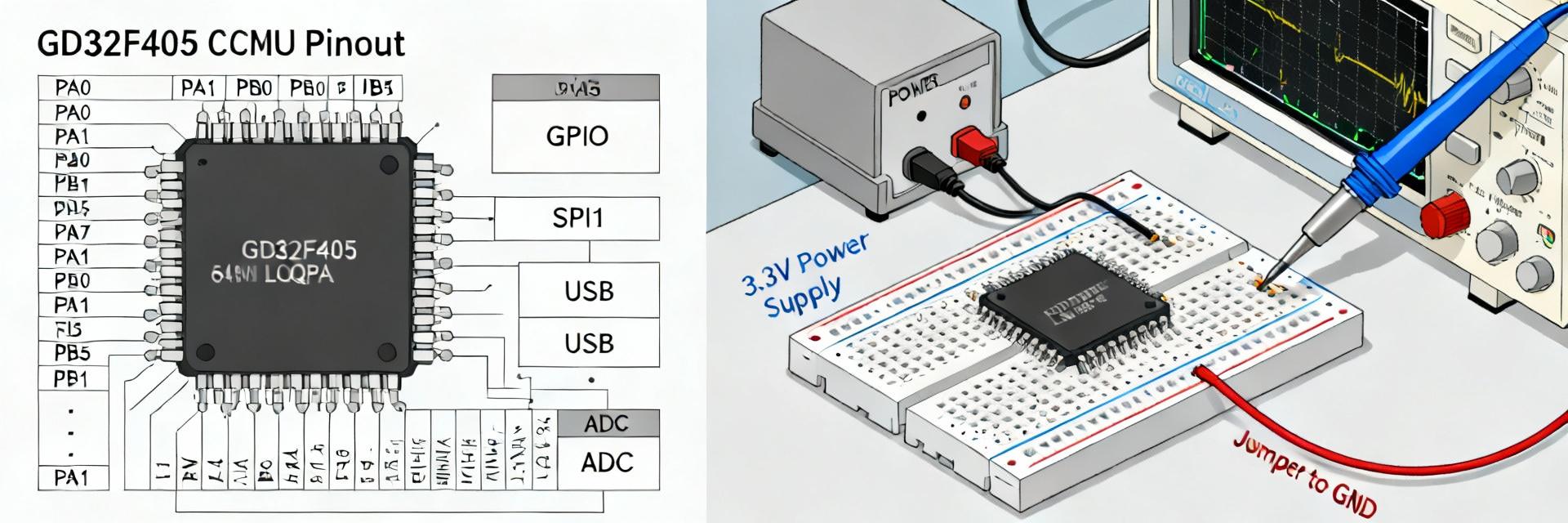
Figure 1: GD32F405RGT6 System Architecture & Integration
Complete Specs Breakdown (Datasheet Deep Dive)
Electrical & Memory
Reliable operation depends on observing voltage envelopes. The device operates from a 2.6–3.6 V domain (3.3 V recommended). It supports internal RC sources and external crystals feeding a PLL. Flash is organized in linear sectors; SRAM includes core RAM plus retention/backup areas. Proper wait-state configuration is mandatory for high-frequency operation.
Peripherals & I/O
The family provides multiple USART/UART, SPI, and I2C controllers. It includes 12-bit ADCs with DMA support, a 2-channel DAC, and a sophisticated suite of timers (Advanced/PWM) for motor control. USB OTG FS and Ethernet MAC (10/100) are available for robust connectivity.
Pinout, Packaging & Reference Maps
Pro Tip: Priority should be given to signals requiring dedicated timing or analog purity (ADC inputs) before assigning general GPIO to multiplexed alternate function (AF) pins.
Benchmarks & Real-World Performance
Core workloads depend heavily on compiler optimization (-O3) and FPU hardware flags. Always validate real-time constraints and interrupt service routine (ISR) latencies using hardware cycle counters.
Design Checklist & Best Practices
Hardware Layout
- Place 10 μF bulk caps near the voltage regulator.
- Route analog traces away from high-speed digital clocks.
- Keep crystal traces short with ground guard rings.
Firmware Management
- Initialize clocks early: HSE/HSI → PLL → Core.
- Enable Flash prefetch and instruction caches.
- Implement flash wear-leveling for frequent data writes.
FAQ: Common Questions
Is the GD32F405RGT6 suitable for motor control applications?
What are the key constraints to check before finalizing a PCB?
How should I reproduce benchmark numbers safely?
