

GD32F405VGT6 Technical Report: Key Specs & Benchmarks
GD32F405VGT6 Technical Report: Key Specs & Benchmarks
This report examines a high-performance 32-bit microcontroller built around a 168 MHz Cortex-M4 core with abundant on-chip memory and extensive peripherals.
Datasheet-class specifications list a 168 MHz core, 1 MB Flash, and 192 KB SRAM, supporting compute-heavy control loops and DSP processing.
Reproducible benchmark templates and integration checklists assist engineering teams in validating performance against real application targets.
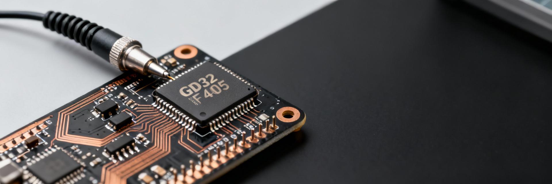
Background & Target Applications
The device targets demanding embedded domains where deterministic compute and rich I/O matter. Applications require a mix of sustained CPU cycles, low-latency ADC sampling, and multi-protocol communications.
Industrial Control
Focus: CPU throughput, large Flash, CAN, and ADC precision.
Motor Control
Focus: FPU/DSP, high-resolution PWM, and fast ADC sampling.
High-speed Sensors
Focus: Multiple ADC channels, DMA, and precise clocking.
USB Gateways
Focus: USB OTG, multiple UART/SPI/I2C, and buffer memory.
MCU Family Positioning & Differentiators
This MCU sits in the Cortex-M4 performance tier offering floating point and DSP instruction support. Hardware FPU and SIMD-like DSP instructions reduce cycle counts for filters and math-heavy tasks compared with baseline M0/M3-class parts.
Key Specs & Architecture
| Field | Value | Design Implication |
|---|---|---|
| CPU | 168 MHz Cortex-M4-class | Ideal for DSP + control; plan CPU budget for FPU context saves |
| Flash | 1 MB | Partition bootloader, primary app, fallback and OTA image |
| SRAM | 192 KB | Reserve for RTOS, stack per task, and DMA buffers |
| Boot Options | Vector table relocation | Enable safe firmware update workflows (ROM/Flash) |
Benchmarks & Measured Performance
Synthetic Throughput (Normalized Score)
Real-world Benchmarks
- USB OTG: Measure bulk throughput and CPU load.
- ADC+DMA: Timer-triggered 4-channel sampling.
- CAN: N-message bursts to check missed frames.
- SPI: Burst 1 MB transfers for DMA throughput.
Metric Recording
Capture average, maximum, and minimum latencies along with CPU utilization and power draw. Documentation of compiler flags (-O2/-Ofast) and cache settings is essential for reproducibility.
Integration & Design Checklist
Hardware Considerations
- ✔ Must: Place VDDD decoupling caps near core pins and ensure a proper ground plane.
- ✔ Have: 8–25 MHz crystal for accurate USB timing and low jitter.
- ✔ Optional: Thermal vias under LQFP100 package for high-power scenarios.
Firmware Best Practices
- ⚡ Configure RTOS heap/stack values conservatively to avoid overflow.
- ⚡ Enable FPU context saving and check vector alignment for RTOS stability.
- ⚡ Implement safe bootloaders with CRC/Signature image validation.
When to select GD32F405VGT6
If Real-time DSP + Multiple Comms → Choose this MCU | If Ultra-low Power → Choose Lower-tier Part | If Extreme Multi-core → Consider Higher SoC
Frequently Asked Questions
What package options and pin count exist for this MCU? +
How should I structure flash partitions for updates? +
What are best practices for minimizing ADC latency? +
