

GD32F407RET6 Datasheet Deep Dive: Key Specs & Pinout
The GD32F407RET6 is a performance-oriented ARM Cortex-M4 MCU family member aimed at connectivity, motor control, and high-throughput embedded designs. This deep dive turns datasheet numbers into actionable design decisions.
Performance Core
Cortex-M4F core delivering high-performance real-time tasks with an integrated FPU for complex control loops.
Memory Density
Abundant SRAM and Flash resources to support RTOS, DMA-driven I/O, and substantial firmware stacks.
Background: what the GD32F407RET6 is and where it fits
Device family & core capabilities: The GD32F407 series is positioned as a general-purpose Cortex‑M4F MCU with DSP extensions. The datasheet lists an ARM Cortex‑M4 core with single‑precision FPU. This combination targets motor control, audio processing, and multi‑bus connectivity where floating‑point and deterministic ISR response matter.
Key package and pin-count summary: The RET6 suffix identifies the LQFP‑64 package variant. It balances I/O count and PCB footprint for mid‑range designs where 48–50 usable GPIOs are typical after accounting for power and debug pins.
Key electrical specs & performance
Memory & CPU
Flash and RAM define firmware size and runtime headroom. 512 KB flash and 192 KB SRAM translate to sufficient space for bootloader+app, RTOS heaps, and stack; the FPU lowers signal processing latency versus integer‑only cores.
Power & Thermal
VDD range (2.6–3.6 V) recommended around 3.3 V. Designers should budget for tens of mA at full speed and microamp sleep modes. Follow decoupling recommendations to avoid transient resets under DMA bursts.
Pinout & package: how to read, interpret, and use the pin map
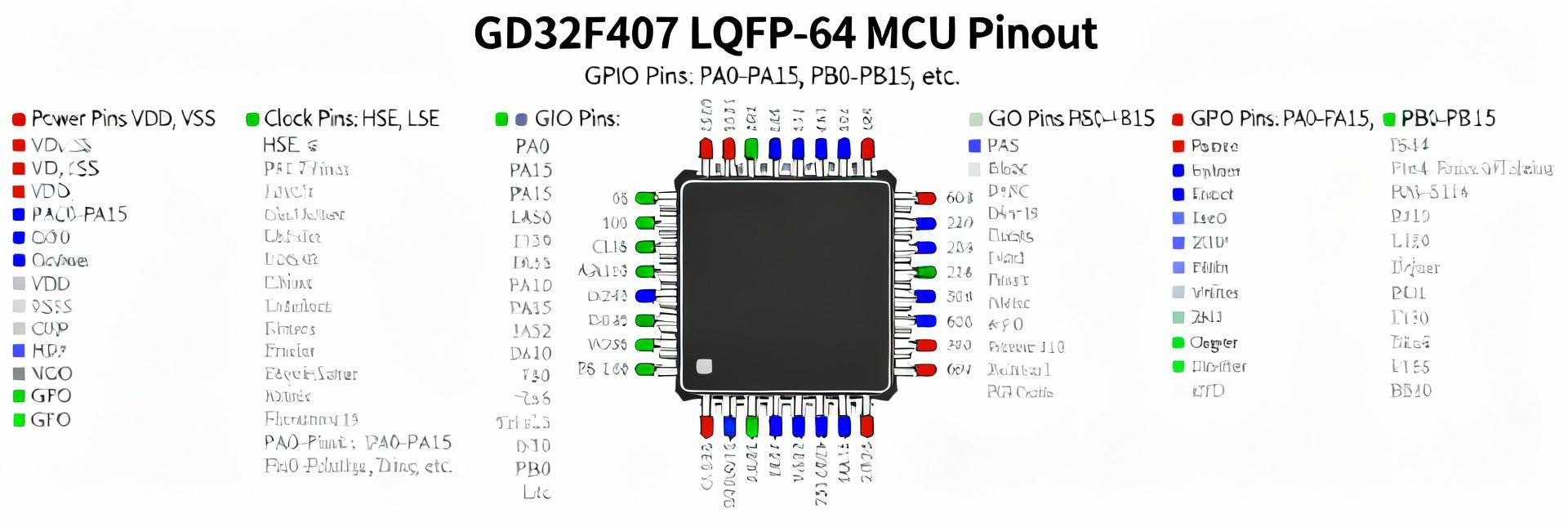
LQFP-64 pin map overview: Grouping pins by function simplifies board planning. Prioritize power (VDD/VSS) and debug pins (SWD), allocate ADC and VREF pins away from noisy digital traces, and reserve SWD for bring‑up.
Pro Tip: Check Alternate Function (AF) tables early—e.g., UART on PA2/PA3—to avoid assigning high‑speed SPI + ADC to shared pins without verifying DMA channel availability.
Alternate functions and multiplexing rules: AF multiplexing creates pin conflicts if not planned. The alternate function tables enumerate AF mappings per pin and list remap constraints.
Peripherals & interfaces
- Communication: USARTs (3+), SPIs, I2Cs, CAN controller, and USB FS device interface. Use SPI with DMA for high sensor throughput.
- Timers & Analog: Advanced timers for PWM with complementary outputs, 12‑bit ADC with multiple channels, and multiple DMA streams.
- Processing: Integrated FPU for fast control math and filtering, essential for BLDC motor control.
Typical applications & design examples
Application Profiles
Ideal for IoT Gateways (USB/UART), BLDC Motor Control (Advanced Timers), and Data Loggers. For ultra-low power, evaluate power-down modes carefully.
Minimal BOM
Include 0.1µF decoupling caps, 10k reset resistor, USB ESD protection, and an 8–25 MHz crystal for stable operation.
Practical PCB integration & bring-up checklist
Layout & Integrity
- Place decouplers within 1–2 mm of supply pins.
- Route analog traces away from high‑speed buses.
- Stitch ground with vias for thermal management.
First-time Bring-up
- Verify 3.3 V rail and check BOOT0/NRST states.
- Connect SWD and flash a simple "Blinky" program.
- Validate peripheral clocks before enabling DMA.
Summary
- The GD32F407RET6 combines a Cortex‑M4F at 168 MHz with 512 KB flash, perfect for connectivity and DSP tasks.
- LQFP‑64 provides a practical balance of size and I/O; plan Alternate Functions early to avoid conflicts.
- Strictly follow datasheet guidance for decoupling and DMA mapping to ensure system stability.
Frequently Asked Questions
