
GD32F407ZKT6 MCU: Performance Metrics & Specs Deep Dive

GD32F407ZKT6 MCU: Performance Metrics & Specs Deep Dive

2026-01-28

This deep dive frames the primary dimensions engineers use to evaluate embedded compute: CPU throughput, memory bandwidth, peripheral latency, and power/performance trade-offs. The GD32F407ZKT6 combines an ARM Cortex-M4 core with FPU/DSP extensions, targeting firmware engineers, hardware designers, and system architects with actionable metrics and deployment microbenchmarks.

To assess real-world performance, we synthesize datasheet specifications, microbenchmarks, and test guidance. Measured metrics include CoreMark/Dhrystone, SRAM/flash latency, DMA throughput, and sustained throughput under interrupt and peripheral load. Readers will gain test plans, tuning steps, and validation criteria tailored for performance-sensitive MCU projects.

Background: GD32F407ZKT6 at a Glance
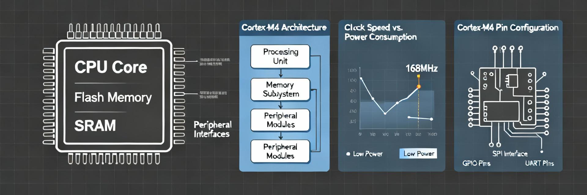
GD32F407ZKT6 MCU Overview

Core Architecture & Silicon Highlights

The silicon implements an ARM Cortex-M4-class core with single-precision FPU and DSP instruction extensions, delivering a balance of integer and floating-point capability. The FPU accelerates common signal-processing kernels and reduces cycle counts per FLOP versus software emulation. For integer tasks, expect strong deterministic ISR latency; for floating-point compute-bound workloads, the hardware FPU yields large throughput gains when code is vectorized properly.

Memory, Packages, and I/O Footprint

Key on-chip resources govern buffering and DMA strategies: integrated flash and multi-kilobyte SRAM banks and multiple package options constrain pin count and peripheral routing. Available interfaces include USART, SPI, I2C, timers, ADC channels, and Ethernet MAC in some variants; package choices determine maximum accessible I/O. Choose larger packages when sustained DMA and external memory interfacing are required; smaller LQFP variants suit constrained I/O but limit buffer sizes.

Key Performance Metrics: Analysis

CPU Throughput & FPU

Measure CoreMark, Dhrystone, MIPS, cycles per interrupt, and FPU FLOPS. Reporting in ops/sec and cycles/op allows for platform scaling comparisons. Build a test plan with consistent compiler flags to reveal real-time headroom.

Integer WorkloadOptimized

Memory Subsystem

SRAM read/write latency, flash execute-in-place timing, and DMA throughput determine data movement. Tune DMA burst sizes and prioritize bus masters to minimize ISR-induced stalls on the memory bus.

DMA BandwidthPeak Capacity

Microbenchmarks & Real-world Tests

Synthetic Benchmarks

Establish baselines using standard workloads like CoreMark and Dhrystone. Run benchmarks at multiple clock frequencies, enforce ISR disabling for pure throughput runs, and record build flags. Document pitfalls like background DMA and peripheral interrupts that skew results.

Application-level Scenarios

Validate with scenario tests: motor control loop latency, FFT throughput for audio, and TCP/IP stack performance. Use cycle counters and logic analyzer traces to surface integration-level limits where DMA contention or bus arbitration become bottlenecks.

Design & Integration Guide

Power & Thermal Management

Peak clock improves throughput but increases power and junction temperature. Tune PLL multiplier settings and voltage scaling. Only use modest overclock margins with verified thermal dissipation and monitored Vcore levels.

Firmware Optimization

Use DMA chains, zero-copy buffering, and interrupt coalescing to maximize throughput. Structure DMA pipelines and assign NVIC priorities intentionally, preferring bare-metal for tight loops or RTOS for complex concurrency.

Comparative Case Studies

GD32F407ZKT6 vs. Comparable Cortex-M4 MCUs

Normalize comparisons by clock-performance, memory footprint, and power. Charts highlighting performance-per-watt and performance-per-dollar help call out where the MCU excels or requires compromise in system design.

Project Example: High-Speed Data Acquisition

A typical flow involves streaming ADC samples into SRAM via DMA, applying DSP kernels, and transmitting via Ethernet. Optimizations like double buffering and increasing DMA burst sizes are critical to quantify headroom and minimize jitter.

Technical Specification Matrix

Specification Item Value / Capability
Core Architecture ARM Cortex-M4 with single-precision FPU
Flash Memory Up to 1 MB (variant-dependent)
SRAM Capacity Up to 192 KB across banks
Max Clock Speed Up to 168 MHz class
Peripherals USART, SPI, I2C, TIM, ADC, DAC, Ethernet MAC
Package Options LQFP and high-pin-count packages

Summary

  • • The GD32F407ZKT6 combines a Cortex-M4 compute core with FPU/DSP extensions, making it suitable for mixed integer and floating-point workloads in embedded MCU designs focused on throughput and latency.
  • • Measure CPU throughput, memory latency/bandwidth, and DMA behavior under representative loads; tune DMA burst sizes and bus priorities to maximize sustained performance.
  • • Validate thermal and power margins, use telemetry for runtime alerts, and follow an iterative measure→isolate→optimize loop before large-scale deployment.

Frequently Asked Questions

How to interpret benchmark results for the GD32F407ZKT6? +
Interpret results by normalizing to clock and considering background bus activity; report ops/sec and cycles/op, and record build flags, interrupts enabled, and DMA state. Compare integer and FP kernels separately, and include memory-bound tests to reveal bottlenecks beyond raw CPU capability.
What microbenchmarks reveal DMA limitations on this MCU? +
Run sequential and random memory transfer microbenchmarks of varying block sizes while toggling concurrent peripheral activity. Look for throughput knee points where small transfers or high contention drop effective bandwidth, and tune transfer sizes and arbitration priorities accordingly.
Which firmware strategies most improve real-time performance? +
Prioritize DMA pipelines with double buffering, minimize ISR work by scheduling processing in threads or post-DMA handlers, align buffers to peripheral burst sizes, and use hardware accelerators when available. Carefully assign NVIC priorities and validate under full peripheral load to ensure real-time guarantees.