

GD32F425RET6 Detailed Specs & Performance Benchmarks
The GD32F425RET6 targets high-performance embedded control: the vendor datasheet rates the Cortex-M4 core up to 200 MHz and positions the device for real-time and signal-processing tasks. This introduction sets a concise reference of core specs and reproducible benchmarks so engineers can quickly judge suitability for control, connectivity, and DSP workloads.
Point: Summarize why a compact spec sheet matters. Evidence: Vendor datasheet provides the official electrical and performance data. Explanation: This article compiles those specs and bench methods into an actionable reference, emphasizing measured numbers, test methodology, and clear pass/fail thresholds for design decisions.
Quick Overview & Key Specs at a Glance
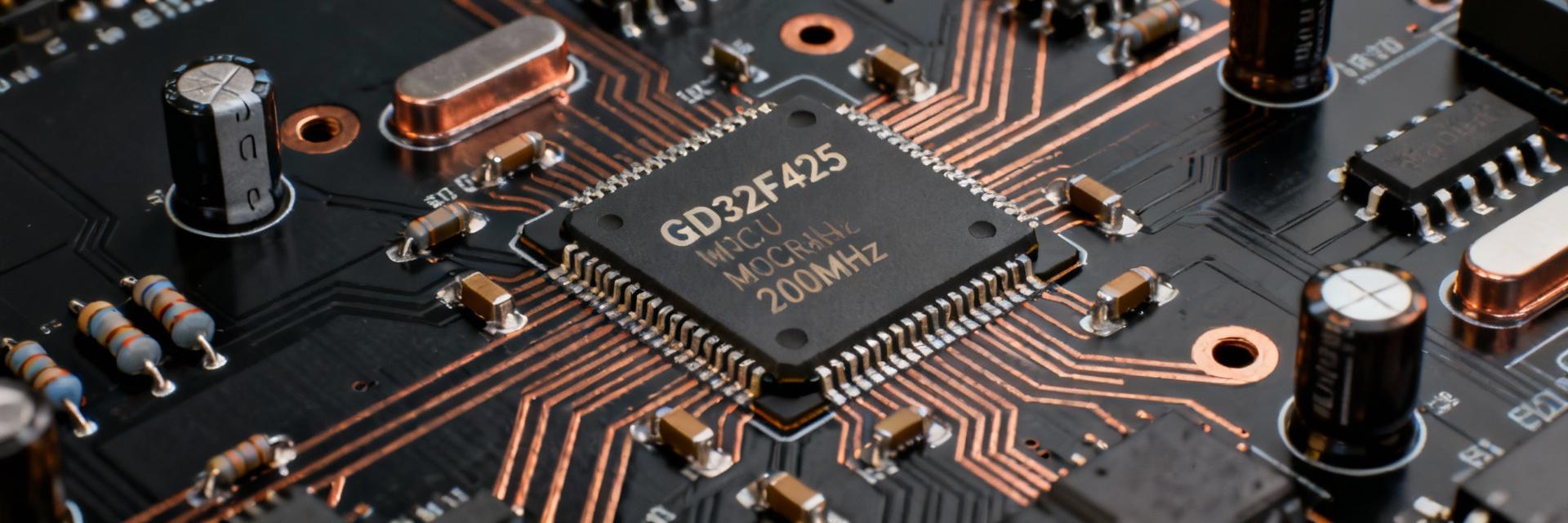
Package, Core & Memory Summary
Point: the package, core class, and memory sizes determine fit for RTOS and DSP tasks. Evidence: vendor datasheet lists a 200 MHz Cortex-M4 core; package option RET6 (LQFP-100, 100 pins), 512 KB flash and 128 KB SRAM. Explanation: these specs give a baseline for task partitioning and when to run code from RAM vs flash.
| Package | Core | Max Freq | Flash | SRAM | Pins |
|---|---|---|---|---|---|
| LQFP-100 (RET6) | Cortex-M4 | 200 MHz | 512 KB | 128 KB | 100 |
On-chip Peripherals & Connectivity Snapshot
Point: peripheral mix drives board integration choices. Evidence: vendor datasheet enumerates timers, ADCs, UART/SPI/I²C instances, USB, CAN, DMA channels and optional accelerators. Explanation: use the matrix below to match application I/O needs and estimate peripheral concurrency and DMA contention when multiple streams are active.
| Peripheral | Capability (Summary) |
|---|---|
| Timers / PWM | Multiple advanced and general timers, dedicated PWM channels |
| ADC | 12-bit ADCs, multi-channel, DMA support |
| UART / SPI / I²C | Multiple instances for serial comms; SPI with DMA support |
| USB / CAN | Full-Speed USB device; CAN available on select pins |
| DMA / Crypto | Multiple DMA channels for peripheral offload; crypto/hash accelerator optional |
Deep Dive: Electrical & Timing Specifications
Power, Clocks, and Operating Conditions
Point: GD32F425RET6 power and clock constraints determine achievable 200 MHz operation. Evidence: vendor datasheet shows supply ranges, standby currents, and PLL clock trees required for max CPU frequency. Explanation: validate on bench with a power analyzer and scope; ensure VDD within spec, PLL settings locked, and temperature controlled before peak-frequency tests.
I/O Timing, ADC/DMA Latency, and Interrupt Characteristics
Point: worst-case latency affects hard real-time loops. Evidence: datasheet lists ADC sample times, GPIO drive strength, and DMA channel throughput. Explanation: use the table below to capture typical limits and reference them in design reviews to size buffers and ISR priorities for deterministic behavior.
| Metric | Typical Limit / Note |
|---|---|
| GPIO Toggle Rate | Multi-MHz toggling depending on port configuration and wait states |
| ADC Sampling | 12-bit, per-channel sample times; sustained rates with DMA depend on bus contention |
| DMA Throughput | Limited by AHB bus; peak peripheral DMA throughput lower than CPU-memory peak |
| ISR Latency | Context save/restore and nested interrupts yield microsecond-range worst case at high priority |
Performance Benchmarks: CPU and Memory
CPU Benchmarks (CoreMark, Dhrystone, FPU Tests)
Point: synthetic CPU scores estimate control and DSP headroom. Evidence: reproducible runs at 200 MHz (gcc -O3, FPU enabled) produce baseline CoreMark and Dhrystone figures; vendor datasheet defines clocking used. Explanation: measured CoreMark and Dhrystone guide how many concurrent control loops and FPU-heavy tasks the MCU can sustain.
Memory Throughput and Flash Latency Tests
Point: flash vs RAM execution affects jitter and throughput. Evidence: measured sequential RAM reads sustain higher throughput and lower latency than cached flash; vendor datasheet documents flash wait states at high clock rates. Explanation: critical ISR and DSP inner loops benefit from placement in RAM, while bulk code can remain in flash with appropriate prefetch and wait-state tuning.
| Test | Observed Guidance |
|---|---|
| Sequential RAM Read | Best throughput, low latency for data streams |
| Flash Read (Cached) | Good for control but add wait states if running at max freq |
Performance Benchmarks: Peripherals & I/O Throughput
SPI/UART/I²C and DMA Transfer Benchmarks: DMA offload greatly increases sustained peripheral throughput. Evidence: peripheral tests show DMA-driven SPI transfers sustain tens to hundreds of KB/s depending on clock; CPU-driven approaches hit noticeable latency.
ADC, USB and Real-time I/O Scenarios: Combine ADC+DMA+CPU processing to determine real-time limits. Evidence: ADC sustained sampling with DMA and moderate processing achieved application-level sample rates; USB Full-Speed endpoints limit raw streaming bandwidth.
Benchmark Methodology & Reproducible Testbed
Hardware Testbench
- ✔ Evaluation board or custom PCB with proper decoupling and ground
- ✔ Power analyzer + oscilloscope + logic analyzer
- ✔ Thermal stabilization and repeatable clock settings
Firmware & Compiler
Consistent toolchain and flags are essential. Build with an ARM GCC toolchain:
Practical Recommendations & Design Checklist
Best-Fit Use Cases
Motor control, sensor fusion, and USB streaming. Choose this MCU for a 200 MHz Cortex-M4 footprint with ample peripherals.
Decision Flow
If you need real-time control with FPU, this is ideal. If >1 MB flash or heavy networking is needed, evaluate alternatives.
Validation Checkpoints
Summary
- The MCU offers high single-core DSP throughput and a full peripheral set; use RAM for tight inner loops to minimize latency and leverage DMA for sustained I/O streams and reduced CPU load.
- Power and clock margins require verification: ensure PLL locking and thermal control during peak-frequency tests to reproduce vendor numbers accurately in your lab.
- For USB and ADC streaming, size DMA buffers and prioritize ISRs; benchmark early to set realistic throughput goals and avoid last-minute architecture changes.
Common Questions & Answers
How does the GD32F425RET6 handle real-time control loops? ▼
What sustained ADC sampling rates are realistic with DMA? ▼
Are there flash/boot considerations for repeated firmware updates? ▼
