

GD32F425VGT6 Datasheet Breakdown: Key Specs & Benchmarks
Datasheet figures and independent benchmarks determine whether an MCU meets real-time, connectivity and low-power targets. This article converts the GD32F425VGT6 datasheet into an actionable spec checklist and a reproducible benchmark plan so engineers can decide quickly whether the part fits a design, which numbers to verify, and how to test them in a lab.
Readers will get a clear spec summary, the datasheet items that actually affect system-level decisions, step‑by‑step benchmark methods (synthetic and peripheral), and concrete integration recommendations for PCB, power and firmware. Where numbers are required, the article points to the exact datasheet tables or figures to cite when finalizing a design.
01 Architecture & Package Overview — Why the Chip Matters
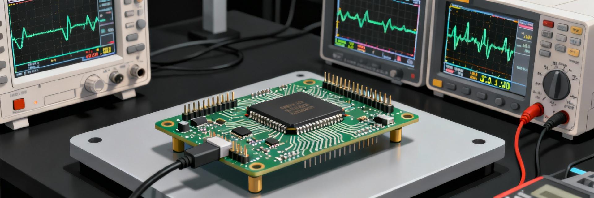
The GD32F family positions high single‑core DSP/MCU performance with Cortex‑M core features and ample connectivity for industrial and consumer applications. For system architects, the core type, FPU availability and maximum core clock determine compute headroom for control loops, crypto or floating‑point signal processing; memory interface and bus widths determine DMA throughput and cache behavior.
Core, instruction set and performance envelope
Point: The core type and max clock set expectations for integer and floating‑point performance.
Evidence: Consult the datasheet core block and Table indicating max SYSCLK (see datasheet, Table "Clock and Reset", p.10).
Explanation: With an M4 core and an FPU, DSP‑style workloads (FFT, PID math) benefit from hardware floating point.
Package variants, pinout and memory footprint
Point: Package selection affects routing, thermal dissipation and I/O count.
Evidence: The datasheet lists LQFP‑100 and other variants, total I/O count and the on‑chip flash/SRAM figures (see "Pin and Package" and "Memory Map" tables, p.4–6).
Explanation: Choose a package with required USB/SDIO/CAN pins exposed to avoid routing compromises.
02 Electrical, Power and Timing Specifications
Power characteristics inform battery life and thermal design. Use datasheet figures as baseline expectations but validate in the lab with your clock, peripheral load and temperature envelope.
Typical Core Performance Metrics (Estimated)
Supply & Domains
Voltage range and active/low‑power currents determine feasibility for battery‑operated designs. Consult "DC Characteristics" (p.22–26).
Clock & Startup
Oscillator options and PLL limits affect wake latency. Measure wake‑from‑stop latency including PLL lock (p.12–14).
03 Peripherals & Connectivity — Capability and Throughput
| Peripheral Group | Key Features | Design Consideration |
|---|---|---|
| Serial (UART/SPI/I2C) | Max nominal rates per p.40-55 | Use DMA for sustained throughput |
| Analog (ADC/DAC) | High resolution & sampling rates | Verify PWM resolution for motor control |
| Storage (SDIO/USB) | High-bandwidth I/O support | Size circular buffers for data-acquisition |
04 Benchmarks: Reproducible Test Plan
Synthetic CPU (CoreMark/Dhrystone)
- ✔ Build with -O3 optimization and link without semihosting.
- ✔ Disable caches if comparing raw core speed against datasheet.
Peripheral Stress Tests
- ✔ Continuous ADC sampling into circular DMA buffers.
- ✔ Measure CPU utilization under heavy UART/CAN burst loads.
05 Integration Checklist & Design Recommendations
PCB & Thermal Design
Place 0.1µF close to each VDD pin. Use solid ground pours with star points for analog domains. Size thermal vias under the package if sustained high current is expected.
Firmware & Boot
Reserve flash for OTA, enable a two‑stage bootloader with rollback, and initialize clocks deterministically before enabling peripherals.
Summary
- CPU and memory: Verify core clock and flash wait‑state behavior before relying on peak CoreMark figures.
- Power envelope: Measure active and sleep currents under your exact clock and peripheral mix for accurate battery life estimation.
- Benchmarks and integration: Follow the PCB and firmware checklist, and iterate on decoupling and clock configuration to meet targets.
Frequently Asked Questions
What are the most important GD32F425VGT6 specs to verify from the datasheet? +
How should I validate GD32F425VGT6 power consumption in a battery design? +
Which GD32F425VGT6 peripheral throughput tests are most revealing? +
