

GD32F427VET6 Datasheet: Quick Specs & Pinout Summary
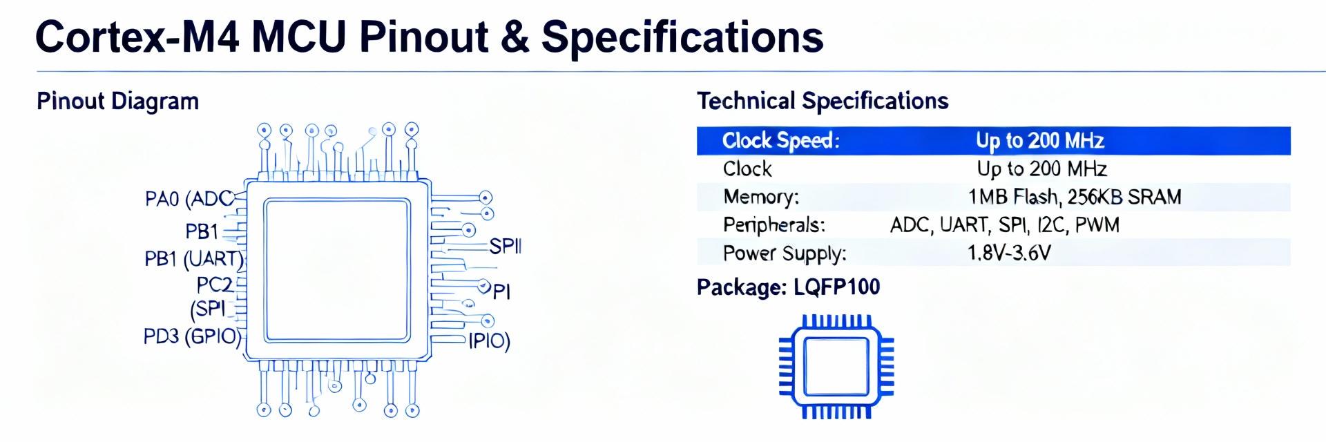
The GD32F427VET6 belongs to the high‑performance Arm Cortex‑M4 MCU class, offering an extensive peripheral set, ample on‑chip memory, and high clock capability. This concise, data‑driven snapshot focuses on core architecture, memory scalability, and package specifications to accelerate your PCB planning and component selection.
Quick Overview & Target Applications
Summary of Part Features
- ✦ Cortex‑M4 core with FPU integration; optimized for high‑performance control and digital signal processing (DSP) tasks.
- ✦ Large on‑chip Flash and SRAM capacity, featuring multicore‑style peripheral density and packages with over 100 pins for extensive I/O capability.
Selection Rationale
Ideal for deterministic real‑time performance requirements. This MCU supports multiple concurrent interfaces (UART, SPI, I2C, CAN, USB) and high ADC/DMA throughput. It is the preferred choice when algorithm complexity and high clock headroom are critical for system responsiveness.
Pinout Summary & Package Guidelines
Functional Pin Grouping
Power and ground pins are strategically clustered—ensure multiple decoupling capacitors are placed near each VDD pin alongside a solid ground plane.
GPIO banks (A, B, C, etc.) are logically grouped. High‑speed interfaces like USB, high‑speed CAN, and specific USART/SPI channels utilize dedicated pins that significantly influence PCB routing. Identify boot configuration and oscillator pins early to prevent signal conflicts.
Package Footprint Tips
The VET6 variant typically utilizes a high‑pin‑count LQFP footprint.
Technical Specification Analysis
Operating Limits
Verify absolute maximum ratings for VDD and I/O tolerance windows. Design considerations must include:
- Budgeting for worst‑case power inrush during startup.
- Accounting for thermal derating based on PCB thermal resistance.
- Following precise decoupling recommendations per VDD pin.
Clocking & Reset
Options include internal RC oscillators and external crystal inputs. Key check items:
- Validate maximum frequency limits for both internal and external sources.
- Analyze startup timing tables for BOR (Brown-out Reset) and POR (Power-on Reset).
- Ensure deterministic timing for peripheral initialization sequences.
Communication Interface Density
| Interface Type | Channel Count | Visual Scale |
|---|---|---|
| USART / UART | 3 – 6 |
|
| SPI | 3 – 5 |
|
| I2C | 2 – 4 |
|
| CAN | 1 – 2 |
|
| USB (Device/OTG) | 1 |
|
Note: Some channels share pins with timers or ADC inputs; verify alternate function mapping early in the design cycle.
Design & Implementation Guide
Pre-Sign-off Checklist
- ✅ Match pinout to required peripherals
- ✅ Confirm VDD/IO sensor tolerances
- ✅ Verify package thermal limits
- ✅ Review EMC/decoupling placement
Common Technical Gotchas
Watch for shared alternate functions, BOR wake-up behaviors, and ADC input multiplexer limitations. The Alternate Function Mapping section of the datasheet is your most critical reference before finalizing SPI/USART timing chains.
PCB Layout & Resource Roadmap
Actionable Layout Items
- Place decoupling caps within millimeters of VDD pins.
- Keep crystal traces shielded and exceptionally short.
- Add thermal vias under power pads to manage heat.
- Segregate analog reference traces from digital noise.
Documentation & Errata
Ensure you have downloaded the Reference Manual and Device Errata. Silicon bugs can alter peripheral behavior—validate your intended features against the errata list before prototyping.
Key Summary
- ✔ High‑performance Cortex‑M4 MCU suitable for complex control and connectivity; always verify exact memory/clock specs for your specific variant.
- ✔ Planning decoupling, oscillator placement, and boot pin assignments early is mandatory to avoid routing conflicts.
- ✔ Review electrical limits and thermal derating to prevent hardware failures and ensure long-term reliability.
Common Questions & Answers
▶ What are the package pinout options for this MCU?
▶ How should I handle boot and reserved pins during design?
▶ What are best practices for ADC and DMA throughput?
