

GD32F450VIT6 Datasheet Deep Dive: Key Specs & Benchmarks
Key Specs, Benchmarks & Professional Implementation Strategies
Mid/high-performance Cortex-M4 MCUs running near 200 MHz often yield 2–3× higher DSP throughput versus typical 120 MHz parts, making them attractive for motor control, audio, and real-time signal tasks.
Learn which datasheet numbers drive system behavior, how to translate clock/memory limits into firmware decisions, and which microbenchmarks validate claims.
Background: Why the GD32F450VIT6 matters for modern embedded designs
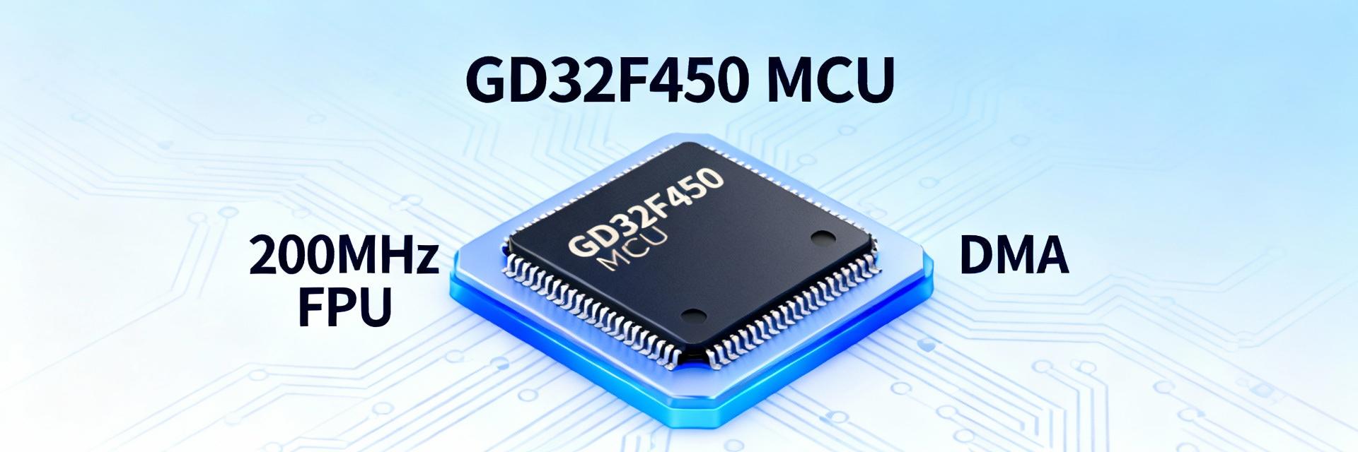
SoC positioning & target applications
The device targets performance-oriented Cortex-M4 use cases such as motor control, advanced sensing, audio processing, and industrial HMI. The combination of a high-clock CPU, single-precision FPU, and rich timer/communication blocks supports control loops and DSP chains. Designers choose this class when integer DSP or floating-point math, tight control latency, and multiple high-speed peripherals are primary system drivers.
Package, supply, and thermal envelope
Package type, operating voltage, and thermal/current limits directly affect PCB layout and cooling choices. The datasheet lists available packages, a defined supply range, and junction/ambient thermal limits that bound continuous throughput. Select package and PCB copper to meet current draw for peripherals and worst-case sustained CPU load to avoid throttling.
Datasheet Key Specs Breakdown
| Feature Category | Key Specifications | Design Impact |
|---|---|---|
| CPU Core | Cortex-M4 (up to 200 MHz) + FPU | High-speed DSP & Math processing |
| Flash/RAM | High-density Flash & multi-bank SRAM | Zero-wait state execution in specific regions |
| Analog Subsystem | 12-bit ADC, DAC, High-speed PWM | Precise motor control and sensor acquisition |
| Connectivity | USB, SPI, I2C, Ethernet, FMC | Versatile industrial & communication bridge |
Benchmarks & Performance Analysis
Core Performance (DMIPS)
Relative performance vs Standard M4 (120MHz)
Real-world Throughput
Microbenchmarks such as sustained SPI DMA transfers, ADC+DMA continuous sampling, and PWM update latency reveal system limits. Document buffer sizes, DMA descriptors, and interrupt load to identify bottlenecks like bus arbitration or flash wait-states affecting DMA servicing.
Design & Firmware Optimization Guide
Clock Tree Tuning
Follow a conservative PLL approach, then adjust flash wait states per the datasheet table to reach higher clocks. Incrementally increase core frequency while validating stability.
Memory Placement
Relocate performance-sensitive routines or buffers to SRAM. Keep tight loops in RAM to avoid flash wait penalties and use inline assembly for critical paths.
Compiler Tweaks
Use aggressive optimization flags for hot loops and tune ISR priorities. Benchmark variance often tracks with code placement and optimization level.
Testing & Validation Checklist
- ✔ Lab Procedures: Measure active/standby current and verify max clock stability under thermal and IO load.
- ✔ Timing Analysis: Confirm flash access timing with logic analyzers and record ambient temperature variance.
- ✔ Reproducibility: Use deterministic input vectors and fixed toolchain settings to ensure repeatable benchmark results.
Case Study: Motor-Control Prototype
Integrating the GD32F450VIT6 in a motor-control prototype required choosing a near-max clock and assigning control loops to FPU-assisted tasks. By partitioning memory for ISR and placing fast control code in SRAM, measured performance met target loop rates with acceptable power. Tradeoffs included slightly increased board copper for thermal headroom.
- Evaluate required CPU/FPU performance vs power budget.
- Verify sustained DMA throughput for sensor streams.
- Confirm package constraints and thermal validation results.
Summary
The datasheet provides CPU/frequency limits and memory maps, but true value comes from mapping those numbers to benchmarks and design choices. Apply these methods to verify claims and optimize firmware for target workloads, closing the loop on GD32F450VIT6 selection.
Use datasheet clock vs. flash wait-state tables to set safe PLL and prescalers.
Place tight loops and sampling buffers in SRAM to minimize flash stalls.
Run CoreMark and report harness details for benchmark reproducibility.
Common Questions
How does the GD32F450VIT6 compare on CoreMark and floating-point throughput? +
What are the most important datasheet fields to validate for clock and thermal stability? +
Which peripheral benchmarks best reveal integration issues on MCU platforms? +
