

Engineers evaluating a high-performance MCU need concise, verifiable numbers. This technical analysis translates GD32H757 datasheet figures into practical guidance for system validation and performance optimization.
DSP & FPU Extensions
Multi-port MAC Support
GD32H757 at a Glance: Datasheet Highlights
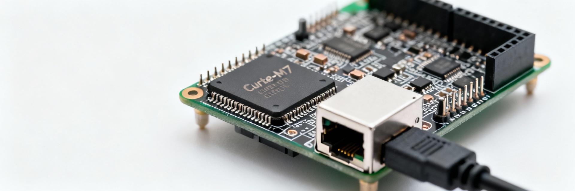
Point: A quick hardware snapshot helps select the right variant. Evidence: The datasheet lists a high-performance Cortex-M7 core, multiple Flash/RAM options, and an extensive peripheral set. Explanation: Treat listed Flash/RAM as configuration choices—verify the specific package option and memory map on your order code before design.
Core Specs (CPU, Clocks, Memory, Flash)
Point: Core capabilities drive system-level performance. Evidence: The CPU targets up to 600 MHz-class operation with caches and DSP/FPU extensions. Explanation: Nominal clock and cache sizes are datasheet-rated; configurable PLLs and flash wait states affect achievable instruction throughput—benchmarks must control clock, wait-state, and cache settings to be comparable.
Integrated Peripherals & Interfaces
Point: Peripherals determine real-world I/O capability. Evidence: High-value peripherals include multi-port Ethernet MAC, USB OTG, multiple SAI/codec interfaces, and CAN-FD controllers. Explanation: Interface maximums (for example CAN-FD nominal bitrates or USB host/device modes) are constrained by PHY and board-level design; confirm PHY selection and clocking to reach datasheet throughput.
Electrical, Power and Thermal Limits
Point: Electrical limits become design constraints. Evidence: The datasheet documents operating voltages, domain-specific currents, and measurement conditions. Explanation: Use those figures as design targets, not guarantees—account for regulator tolerances, peripheral loading, and measurement methodology when budgeting system power.
Power Consumption Profiles & Operating Modes
Point: Power vs. performance trade-offs are explicit. Evidence: Active and standby currents vary by clock, core DVFS-like modes, and peripheral gating. Explanation: Budget power with margin: measure with the same compiler flags and workloads the datasheet used, and expect higher system-level consumption when supporting high-speed PHYs or external memories.
Thermal Characteristics & Package Considerations
Point: Thermal specs set PCB cooling needs. Evidence: Junction-to-ambient thermal resistances (RθJA) are provided per package. Explanation: Select package and PCB copper, add thermal vias, and derate clock or workload under constrained airflow to stay within thermal envelopes.
Benchmarks & Real-World Performance
Point: Benchmarks reveal usable performance beyond raw specs. Evidence: Synthetic integer/FPU scores and I/O throughput tests map to datasheet claims only when test conditions match. Explanation: Synthetic tests show peak compute; application-level tests (network stacks, USB transfers) expose DMA, cache, and bus contention limitations.
Synthetic Benchmarks
Focus on CoreMark and Dhrystone scores. Measure cycles per operation under controlled cache states to compare against the 600 MHz peak frequency.
Application Benchmarks
Evaluate Ethernet UDP/TCP throughput and USB sustained transfer rates. Sustained throughput depends on DMA efficiency and CPU servicing model.
Reproducible Benchmark Methodology
Point: Repeatability requires a strict test plan. Evidence: Differences in compiler flags, clock trees, and warm caches lead to divergent results. Explanation: Define hardware baseline, firmware build flags, clock sources, temperature, and measurement instruments before testing.
Test Environment and Tools
Use a calibrated power analyzer, logic analyzer for bus traces, and network-load generators for Ethernet/USB. Specify supply voltage, regulated clocks, and ambient temperature; record tool resolution and sampling rates.
Measurement Pitfalls and How to Avoid Them
- • Cache Warmup: Always perform "warm-up" runs before recording data.
- • Wait States: Verify Flash access latency settings (WS) match the core clock.
- • Clock Domains: Ensure peripheral clocks are not bottlenecked by APB/AHB dividers.
Design & Integration Best Practices
Power & PCB
Choose regulators with sufficient transient response. Place low-ESR decouplers close to pins. Follow the recommended start-up sequencing to protect Flash and PLLs.
Clocking & Layout
Isolate jitter-sensitive traces and minimize ground loops. Route high-speed PHY traces (Ethernet/USB) per differential pair standards to preserve signal integrity.
Selection Checklist & Action Plan
- [✓] Validate clock, PLL, and flash wait-state settings—these determine if the GD32H757 meets advertised compute throughput.
- [✓] Prioritize DMA and buffer sizing for sustained Ethernet/USB/CAN-FD throughput.
- [✓] Design with thermal margin; package choice and PCB copper affect sustained high-frequency operation.
